Tuesday, June 25th 2013

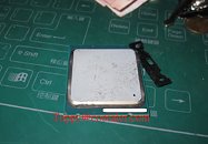
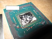
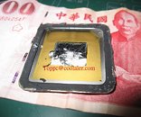
Intel Core i7-4960X De-Lidded
Coolaler.com community member "Toppc" scored an engineering sample of Intel's upcoming Core i7-4960X "Ivy Bridge-E" socket LGA2011 processor, and wasted no time in taking a peek inside its integrated heatspreader (IHS). Beneath the adhesive layer that holds the IHS to the package, which could be fairly easily cut through, "Toppc" discovered that Intel is using a strong epoxy/solder to fuse the processor's die to the IHS, and not a thermal paste, like on Core i7-3770K. Solders tend to have better conductivity than pastes, but make it extremely difficult to de-lid the processors, not to mention potentially disastrous. In the process of delidding this chip, "Toppc" appears to have knocked out a few components around the die. Unless you're good at precision soldering, something like that would be a fatal blow to your $1000 investment.
Source:
Coolaler Forums


12 Comments on Intel Core i7-4960X De-Lidded
Let's hope Ivy-E clocks much better than SB-E now that we know it doesn't come with el cheapo TIM.
Would like to know Intel's excuse for not providing this kind of solution ATLEAST on their K chips on the 1150 platform.
At least now people know what to do in order to pop the top "safely" :)
We know that Intel had thermal issues with SB-e. The proof of this being the 2 lasered off cores on each die.
We know IB experimented with thermal paste, rather than solder. IB had a tendency to run hotter than SB.
Intel isn't that kind of stupid. They chose to use the more expensive solder, because their experiment with paste failed. Of course, they could have discovered this 6 months into the IB 1155 life cycle, and put out an IB-e chip then. Apparently it took another 18 month for Intel to deem it necessary.Let's not go there. The nerfing of x79 was painful enough. The fact that the z87 PCH is better than the x79 in almost everything (yeah, less PCI-e lanes, but that's it) is severely depressing. You tend to get that though when you use a PCH that is based upon 4 year old technology when in came out (Patsburg was 65nm technology as far as I remember).
Also, look back a few days. Haswell-e is slated for release in late 2014. Broadwell will already have moved into the consumer market prior to Haswell-e entering the market.
Edit:
Thinking about this a bit more, it dawns on me. You've got about a 10% increase in CPU performance from SB to IB. You've got another approximately 10% increase from IB to Haswell (they were focusing on the GPU after all). You've therefore got about a 21% increase from SB to Haswell. The amount of overclocking you can do can narrow what gap significantly, assuming that Haswell isn't decked out in DDR4 and the like.
The difference between SB 1155 and Haswell 1150 is largely just a much upgraded PCH and IGP. The 2011 variants of these technologies forgo the IGP for more cores, so you're looking at minor gains in the CPU. The real difference is the PCH, which has been retained from SB-e to IB-e. Maybe Haswell will fix this, but as it stands the x79 disappointment stains anything a modest CPU performance increase can provide.
He probably did it for science and to show that Intel used fluxless solder.
I believe they HAD to use solder on these parts as its a 125W Hex core CPU versus a 77/84W quad. ;)
The point was that Intel had thermal issues. These thermal issues could be caused by one of two issues; either the CPU cores generate too much heat or the heat is not transferred quickly enough from the CPU.
There are two cores lasered off, on that we can agree. This decreases thermal output by having less cores. For the sake of your argument, let's assume this was a manufacturing defect and isn't relevant.
The heat transfer can be affected in one of two ways, interface material or medium transfer. Intel not only didn't package an air cooler with the CPU, their recommendation was for a water cooling system. This means that the heat needs to be dissipated quickly, which means there is a ton being generated. The use of a solder between CPU and its metal casing means that the increased dissipation from the water cooling would not have been enough to allow for the cheaper TIM.
Intel is full of smart engineers. They don't choose a more expensive process just for giggles. Soldering costs money that they aren't willing to spend unless they have to. Economics always trumps the overclocking market.
To the "other" things argument, show me something valid. If you are saying that all 6 cores are bad 8 cores, then why are the dies all setup with the same 2 cores lasered off? To the power consumption aspect, then why are the Xeon 8 cores running off the same power sources, but at lower clocks, in the same thermal envelope? I haven't yet seen a reason that is more feasible than the thermal envelope, though if you can offer one I would gladly consider it.
I'm not sure what you went on about up there. We agree mostly, but it looks like you may have been hung up assuming I meant ALL Hex's are broken octo's. I am just saying its possible as it has been done in the past. That, actually, is how binning works. If a CPU cant make bin A, it goes to bin B. If it cant make bin B, it goes to bin C. Look at the AMD unlocking for an example. Is really it true? Who knows... but it is just as possible. I am sure thermal considerations played a part in it as well. I hope my clarification helps ya out there. :)