Tuesday, November 17th 2015

Intel 7th Generation Core "Kaby Lake" and 200-series Chipset Platform Outlined
Intel's tick-tock product development cycle is disturbed. The cadence of launching a new CPU microarchitecture on a given silicon fab process, miniaturizing it to a smaller fab process, and then launching an even newer micro-architecture on that process; is about to change with the company's 7th generation Core "Kaby Lake" processor. When launched, it would be the third microarchitecture built on the company's 14 nm process, besides "Skylake" (current new architecture) and "Broadwell" (miniaturization of "Haswell" to 14 nm.) Some of the very first documents related to Kaby Lake began to move about, making news along the way. The architecture is scheduled to launch along with its companion 200-series chipset some time in 2016.
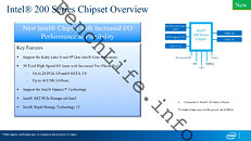
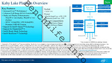
To begin with, Core "Kaby Lake" will continue to be built on the LGA1151 package, and will likely be backwards compatible with existing 100-series chipset motherboards with a firmware update. From what we get to understand from leaked material, it will not be a vastly newer architecture than Skylake, at least not of the kind Skylake was to Broadwell. There are still CPU performance enhancements on offer, an "enhanced full-range BClk overclocking," which could mean improved overclocking on chips with upwards-locked multipliers (although we won't get our hopes too high and call it a return of the BClk overclocking era). A bulk of the R&D will fall into improving the integrated graphics, to support multiple 5K displays, 10-bit HVEC and VP9 hardware-acceleration; platform-integrated Thunderbolt 3, and platform interface support for Intel Optane (3D XPoint memory).Like its predecessor, "Kaby Lake" will feature an integrated memory controller that supports both DDR4 and DDR3 memory. It will support faster DDR4-2400 natively; and DDR3L-1600. DMI 3.0 (physical PCI-Express 3.0 x4) will continue to be the chipset bus. The 200-series chipset, codenamed "Union Point," in its topmost variant, will feature native support for Intel Optane SSDs, and will feature greater port-flexibility among its downstream PCIe lanes. It will feature Rapid Storage Technology support for PCIe storage devices. By the time it launches, NVMe will achieve greater presence in the market.
Since it will be built on the existing 14 nm process, TDP of "Kaby Lake" chips will be similar to existing "Skylake" ones - 35W and 65W for dual- and quad-core desktop chips; with 95W for enthusiast-K variants of the desktop chips. Elsewhere in the lineup, there will be 8 top-level variants of "Kaby Lake," four of which will launch in Q3-2016, and four in early-2017, as incremental lineup upgrades.
Source:
Benchlife.info
To begin with, Core "Kaby Lake" will continue to be built on the LGA1151 package, and will likely be backwards compatible with existing 100-series chipset motherboards with a firmware update. From what we get to understand from leaked material, it will not be a vastly newer architecture than Skylake, at least not of the kind Skylake was to Broadwell. There are still CPU performance enhancements on offer, an "enhanced full-range BClk overclocking," which could mean improved overclocking on chips with upwards-locked multipliers (although we won't get our hopes too high and call it a return of the BClk overclocking era). A bulk of the R&D will fall into improving the integrated graphics, to support multiple 5K displays, 10-bit HVEC and VP9 hardware-acceleration; platform-integrated Thunderbolt 3, and platform interface support for Intel Optane (3D XPoint memory).Like its predecessor, "Kaby Lake" will feature an integrated memory controller that supports both DDR4 and DDR3 memory. It will support faster DDR4-2400 natively; and DDR3L-1600. DMI 3.0 (physical PCI-Express 3.0 x4) will continue to be the chipset bus. The 200-series chipset, codenamed "Union Point," in its topmost variant, will feature native support for Intel Optane SSDs, and will feature greater port-flexibility among its downstream PCIe lanes. It will feature Rapid Storage Technology support for PCIe storage devices. By the time it launches, NVMe will achieve greater presence in the market.
Since it will be built on the existing 14 nm process, TDP of "Kaby Lake" chips will be similar to existing "Skylake" ones - 35W and 65W for dual- and quad-core desktop chips; with 95W for enthusiast-K variants of the desktop chips. Elsewhere in the lineup, there will be 8 top-level variants of "Kaby Lake," four of which will launch in Q3-2016, and four in early-2017, as incremental lineup upgrades.


47 Comments on Intel 7th Generation Core "Kaby Lake" and 200-series Chipset Platform Outlined
-no USB 3.1.
-still supporting DDR3L (Skylake motherboards seem to be few and far between).
-enthusiast processors are 95W TDP instead of 91W
I'm pretty happy I didn't wait for Kaby Lake.
- USB 2.0 in 2015 (almost 2016). Daym.
- what will they improve with CPU's when 6700K is already clocked so high only way they can make it better is to add more cores or drastically improve IPC. Which I highly doubt it'll happen.
- lastly, zero actual new innovations
AMD, get that Zen out and kick Intel in the lazy ass. This is getting ridiculous.
Plus AMD proved with HSA that iGPU can speed up the tasks which would normally use only CPU part of the APU.
This is why it's in everyone's best interest that AMD puts up a decent if not competitive fight against whatever Intel offers at the time of Zen's release. When AMD puts out their new APUs based on the Zen-architecture, that's when we'll see some impressive performance gaps between them and Intel's IGP for sure.
USB 3.1 gen 2 - Intel wants to sell its Thunderbolt 3.0 chips for this, just as they're doing to Gigabyte and Asus now. If Intel can charge $10 for another chip, why wouldn't they? They're a business after all. It took three years for USB 3.0 to be part of Intel's chipsets if I don't remember wrong and then we got a massive two ports... Expect the same with USB 3.1 gen 2.
Note that these chips won't launch until Q3/Q4 2016, so it's still going to be quite a wait...