Monday, April 3rd 2017

Rumored Intel Kaby Lake-G Series: Modular, Multi-Die, HBM 2, AMD Graphics IP?
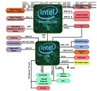
Rumors have been making the rounds about an as-of-yet unannounced product from Intel: a Kaby Lake-G series which would mark Intel's return foray to a multi-chip module in a singular package. The company has already played with such a design before with its Clarkdale family of processors - which married a 32 nm CPU as well as a 45 nm GPU and memory controller in a single package. Kaby Lake-G will reportedly make away with its simple, low-data rate implementation and communication between two parts, instead carrying itself on the shoulders of Intel's EMIB (Embedded Multi-die Interconnect Bridge), which the company claims is a "more elegant interconnect for a more civilized age."
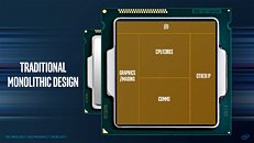
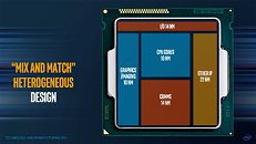
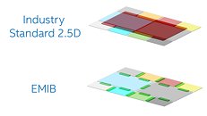
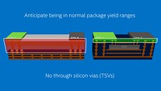
Instead of using a large silicon interposer typically found in other 2.5D approaches (like AMD did whilst marrying its Fiji dies with HBM memory), EMIB uses a very small bridge die, with multiple routing layers, which provide a good measure of price/data paths for the interconnected, heterogeneous architecture. This saves on the costly TSV (Through-Silicon Vias) that dot the interposer approach.For now, rumors peg these Kaby Lake-G as special BGA processors based on Kaby Lake, with an additional discrete GPU on the package. The TDP of these processors (at 65 W and 100 W) is well above the Kaby Lake-H's known 45 Watts. Which begs the question: what exactly is under the hood? This, including Intel's modular approach to chip design for which it developed its EMIB technology, could probably account for the AMD graphic's chip TDP - a discrete-level GPU which would be integrated on-die, EMIB's routing layers handling the data exchange between GPU and processor. This is where HBM 2 memory integration would also come in, naturally - a way to keep a considerable amount of high-speed memory inside the package, accessible by the silicon slices that would need to. Nothing in the leaked information seems to point towards this HBM 2 integration, however.Also helping these "AMD Radeon IP integration" story (besides TDP) is that the two chips that will be part of the Kaby Lake-G series will feature a package size of 58.5 x 31mm - bigger than a desktop Kaby Lake-S (37.5 x 37.5 mm) and the Kaby Lake-H series chips (42 x 28mm). The extra space would accommodate increased footprint of the GPU package - though for now, leaked information points only, again, to Intel's own GT2 graphics solution, though Benchlife seems to put much stock on the AMD side of the equation.The heterogeneous, modular approach to CPU development here would really benefit Intel thusly: it would allow it to integrate such external graphics solutions that could be produced in other factories entirely and then fitted onto the package; would allow Intel to save die space on their 10 nm dies for actual cores, increasing yields from their 10 nm process; and would allow Intel to recycle old processes with new logic inside the CPU package, permitting the company to better distribute production load across different processes, better utilizing (and extracting value from) their not-so-state-of-the-art processes.
If Intel advances with this modular approach, we stand to see some really interesting designs, with multiple manufacturing processes working in tandem inside a single package, giving Intel more flexibility in developing and implementing its fabrication processes. What do you think about this take on CPU development?
Sources:
BenchLife, Computerbase.de
Instead of using a large silicon interposer typically found in other 2.5D approaches (like AMD did whilst marrying its Fiji dies with HBM memory), EMIB uses a very small bridge die, with multiple routing layers, which provide a good measure of price/data paths for the interconnected, heterogeneous architecture. This saves on the costly TSV (Through-Silicon Vias) that dot the interposer approach.For now, rumors peg these Kaby Lake-G as special BGA processors based on Kaby Lake, with an additional discrete GPU on the package. The TDP of these processors (at 65 W and 100 W) is well above the Kaby Lake-H's known 45 Watts. Which begs the question: what exactly is under the hood? This, including Intel's modular approach to chip design for which it developed its EMIB technology, could probably account for the AMD graphic's chip TDP - a discrete-level GPU which would be integrated on-die, EMIB's routing layers handling the data exchange between GPU and processor. This is where HBM 2 memory integration would also come in, naturally - a way to keep a considerable amount of high-speed memory inside the package, accessible by the silicon slices that would need to. Nothing in the leaked information seems to point towards this HBM 2 integration, however.Also helping these "AMD Radeon IP integration" story (besides TDP) is that the two chips that will be part of the Kaby Lake-G series will feature a package size of 58.5 x 31mm - bigger than a desktop Kaby Lake-S (37.5 x 37.5 mm) and the Kaby Lake-H series chips (42 x 28mm). The extra space would accommodate increased footprint of the GPU package - though for now, leaked information points only, again, to Intel's own GT2 graphics solution, though Benchlife seems to put much stock on the AMD side of the equation.The heterogeneous, modular approach to CPU development here would really benefit Intel thusly: it would allow it to integrate such external graphics solutions that could be produced in other factories entirely and then fitted onto the package; would allow Intel to save die space on their 10 nm dies for actual cores, increasing yields from their 10 nm process; and would allow Intel to recycle old processes with new logic inside the CPU package, permitting the company to better distribute production load across different processes, better utilizing (and extracting value from) their not-so-state-of-the-art processes.
If Intel advances with this modular approach, we stand to see some really interesting designs, with multiple manufacturing processes working in tandem inside a single package, giving Intel more flexibility in developing and implementing its fabrication processes. What do you think about this take on CPU development?

32 Comments on Rumored Intel Kaby Lake-G Series: Modular, Multi-Die, HBM 2, AMD Graphics IP?
I don't think Intel gonna want to feed AMD with Ryzen attacking Intel on all fronts by the end of the year.
$264 Millions annually for the GPU licencing is what Intel is paying Nvidia.
Putting those extra money into AMD pocket would definitely hurt Intel in the long run.
Could also be some 6 core thing for mobile workstations. Or a cheaper way for more L4 cache.
...true but we both know no one could afford for Amd to go out of business for obvious reason with out a suitable replacement. So intel does this jogging in place thing for a couple of years, throws them a life line or two and we have todays current situation. Now intel drops a ridiculous new line they've been sitting on for a stupid price because there is now competition and some excitement in the cpu world. Badda Bing.... Badda Boom...
Nvidia hates Intel.
How hard is it for people to learn it?....
How hard is it for people to learn it?....
That should say something about Nvidia, lol...
And they even get to hide their super expensive but still shitty IGP's while doing it. :D
Along with maximizing revenues from older nodes, the design lends itself to use a variety of graphics chips (possibly from both Intel and AMD) to arrive at a line of products.
I'm not sure how well this would play for AMD though... Just when they will be trying to make a comeback to notebook market, feeding their biggest rival with their own graphics IP, which has been their most valuable asset in that market? Maybe they will only share the IP for their inferior parts? As in for example Polaris, but not Vega yet?
But again, in this market no one wants the other to go belly up, lest they end up a monopoly and have to deal will all sorts of additional regulations.
Just a matter of time till they announce some self driving platform thing.
www-ssl.intel.com/content/www/us/en/automotive/autonomous-vehicles.html
As with anything hardware related, I'll hold off until I can see independent real-world studies, but I have high hopes for this product.
All the AMD deal was for licensing IP that Nvidia forced it to license from itself. Any increase in tdp or die space is likely coming from a larger Iris GPU.