Wednesday, July 5th 2017

NVIDIA Laying Groundwork for Multi-Chip-Module GPUs
Multi-Chip-Module accelerators are nothing new, really. Though there are earlier implementations, when it comes to recognizable hardware most of us has already heard of, these solutions harken back to Intel's Kentsfield and Yorkfield quad-core processors (built on the 65 nm process for the LGA 775 package.) However, a singular issue with this kind of approach is having a powerful, performant-enough interconnect that allows the different cores in each module to really "talk" to each other and work perfectly in tandem. More recently, AMD has demonstrated the advantages of a true MCM (Multi-Chip-Module) approach with its Ryzen CPUs. These result from the development of a modular CPU architecture with a powerful interconnect (Infinity Fabric), which has allowed AMD to keep die size to a minimum (as it relates to a true 8-core design, at least), while enabling the company to profitably scale up to 16-cores (2 MCMs) with Threadripper, and 4 MCMs with Epyc (32 cores.)
AMD has already given hints in that its still long-coming Navi architecture (I mean, we're still waiting for Vega) will bring a true MCM design to GPUs. Vega already supports AMD's Infinity Fabric interconnect as well, paving the way for future APU designs from the company, but also MCM GPU ones, leveraging the same technology. And NVIDIA itself seems to be making strides towards an MCM-enabled future, looking to abandon the monolithic die design approach it has been taking for a long time now.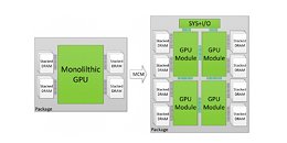

 NVIDIA believes a modular approach is the best, currently technically and technologically feasible solution to a stagnating Moore's Law. CPU and GPU performance and complexity has been leaning heavily on increasing transistor counts and density, whose development and more importantly, production deployment, is slowing down (the curve that seemed to be exponential is actually sigmoidal, eh!). In fact, it is currently estimated that the biggest die-size achievable with today's technology is ~800 mm². The point is driven home when we consider that the company's Tesla V100 comes in at a staggering 815 mm², thus already straining the technical die-size limit. This fact, coupled with the industry's ever-increasing need of ever-increasing performance, leads us to believe that the GV100 GPU will be one of NVIDIA's last monolithic design GPUs (there is still a chance that 7 nm manufacturing will give the company a little more time in developing a true MCM solution, but I would say that odds are NVIDIA's next product will already manifest in such a design.
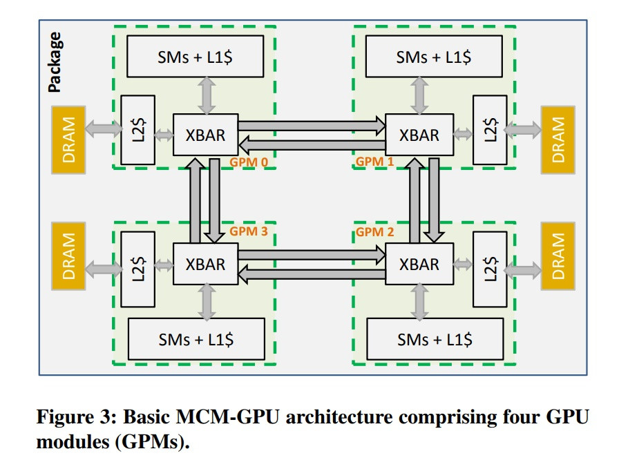
 In a paper published by the company, NVIDIA itself says that the way ahead is towards integration of multiple GPU processing modules in a single package, thus allowing the GPU world to achieve what Ryzen and its Threadripper and EPYC older brothers are already achieving: scaling performance with small dies, and therefore, higher yields... Specifically NVIDIA says that they "(...) propose partitioning GPUs into easily manufacturable basic GPU Modules (GPMs), and integrating them on package using high bandwidth and power efficient signaling technologies." In its white paper, NVIDIA says that "the optimized MCM-GPU design is 45.5% faster than the largest implementable monolithic GPU, and performs within 10% of a hypothetical (and unbuildable) monolithic GPU (...)", and that their "optimized MCM-GPU is 26.8% faster than an equally equipped Multi-GPU system with the same total number of SMs and DRAM bandwidth."
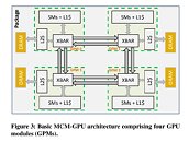 These developments go on to show engineering's ingenuity and drive to improve, and looks extremely promising for companies, since abandoning the monolithic design philosophy and scaling with a variable number of smaller dies should allow for greater yields and improved performance scaling, thus both keeping the high-performance market's needs sated, and the tech companies' bottom line a little better off than they (mostly) already are. Go on ahead and follow the source NVIDIA link for the white paper, it's a very interesting read.
Sources:
NVIDIA MCM Paper, Radar.O'Reilly.com
AMD has already given hints in that its still long-coming Navi architecture (I mean, we're still waiting for Vega) will bring a true MCM design to GPUs. Vega already supports AMD's Infinity Fabric interconnect as well, paving the way for future APU designs from the company, but also MCM GPU ones, leveraging the same technology. And NVIDIA itself seems to be making strides towards an MCM-enabled future, looking to abandon the monolithic die design approach it has been taking for a long time now.


49 Comments on NVIDIA Laying Groundwork for Multi-Chip-Module GPUs
That said, I'm all for MCM because it means higher yields and higher yields means more bang for the buck. My concern/fear is that they'll run into the same problems as SLI/Crossfire where support is spotty.
Smaller nodes will double the cost per chip due to double the number of steps to manufacture , until euv hits mass manufature likely not soon(full euv 9step production not mearly a step or two done with it) , pellicles have yet to be made that are upto the job while all other issues are on the way to resolution they still haven't defined an appropriate material to use that can withstand euv , this is a four year issue at worst.
All this means Nvidia and Amd are going to Have to make small dies work.
Since doing 7Nm and they will, would require massive price rises to accommodate the production cost.
They're all going the way of epyc for a time , small chips in a cluster ,its the only way forward.
Question is who realised it first Amd or Nvidia , epyc ,says Amd but Nvidia could have had this up their sleeves a while too.
It would be epic.
I would wager that MCM in implementation not allow or handle overclock and they are busy finding ways to time everything through on die cache and the cache misses are one of the holdups.
**I'm on mobile and between autocorrect, and fat fingers.....
xD
Direct3D 12 and Vulkan allow draw and compute calls to be sent to multiple GPUs easily, the problem is that how to execute it is not intrinsic to their design. Software developers have to go the extra mile to enable multi-GPU capabilities and the lion's share of them don't.
The only solution is to "fake it until you make it." I just don't know if that is even possible and if it is, there will be drawbacks.
I think the fact they don't use the word "core" to describe these may be telling. If there is, in fact, only one dispatcher that covers all the modules, the dispatcher design limits how many modules can be attached. Certainly fits the "fake it until you make it" approach. Problem is, only benefit is improving yields. Because they give up so much space for each module on the interposer, I doubt these MCM'd chips can keep up with the larger monolithic chips with far more transistors.
I really think advanced AI will come into play like it supposedly does in Ryzen in the GPU domain, to keep MCM on track. All the hardware limitations can be overcome with more transistors and better logic, and maybe the answer is a branch.xml for the future that can be kept in memory to allow hardware agnostic performance so that scenarios can be loaded partially at each major branch and weighted against X number of runs.
As for the dispatcher, one could have a central dispatch core that uses NVLink or infinity fabric to send jobs to a number of cores, with each core having a memory interface and dedicated L1 and L2 memory with access to a shared PCIe link.
Closer cores and a piece of hardware to check the code path in advance and communicate that back through drivers to fetch data from each branch possibility and run unused cycles even if its wasted would still be faster than some of the negative scaling we have seen, and you are correct that if its presented to all games unless they request lower level access and are optimized for it, that it should run as fast if not faster by at least some percent all of the time.
Yet the GP100 is doing just dandy on the HPC market, whilst Vega is enjoyed by a handful of "pioneers".
Hell, look at Intel trying to move up its LGA-20166 mobo and CPU launch by just a few months and the disaster that ended up being with an underprepared and buggy platform launch. And that was an already expected platform launch that was accelerated by just a few months.