Tuesday, June 26th 2018

NVIDIA GV102 Prototype Board With GDDR6 Spotted, Up to 525 W Power Delivery. GTX 1180 Ti?
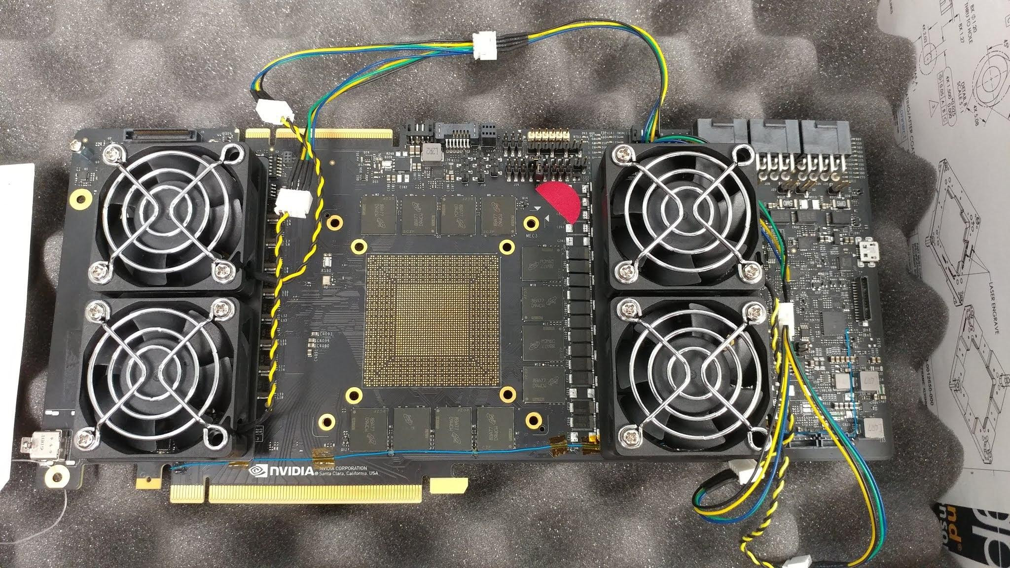
Reddit user 'dustinbrooks' has posted a photo of a prototype graphics card design that is clearly made by NVIDIA and "tested by a buddy of his that works for a company that tests NVIDIA boards". Dustin asked the community what he was looking at, which of course got tech enthusiasts interested.
The card is clearly made by NVIDIA as indicated by the markings near the PCI-Express x16 slot connector. What's also visible is three PCI-Express 8-pin power inputs and a huge VRM setup with four fans. Unfortunately the GPU in the center of the board is missing, but it should be GV102, the successor to GP102, since GDDR6 support is needed. The twelve GDDR6 memory chips located around the GPU's solder balls are marked as D9WCW, which decodes to MT61K256M32JE-14:A. These chips are Micron-made 8 Gbit GDDR6, specified for 14 Gb/s data rate, operating at 1.35 V. With twelve chips, this board has a 384-bit memory bus and 12 GB VRAM. The memory bandwidth at 14 Gbps data rate is a staggering 672 GB/s, which conclusively beats the 484 GB/s that Vega 64 and GTX 1080 Ti offer.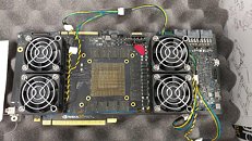 Looking to the top edge of the PCB we see a connector similar to NVIDIA's NVLink connector, but it's missing half of its pins, which means daisy chaining more than two cards won't be possible. Maybe NVIDIA plans to segment NVLink to "up to two" and "more than two", with the latter of course being much more pricey, similar to how server processors are segmented by their multi-processor support. It could also be a new kind of SLI connector, which I'm not sure about, as GPU vendors want to get rid of this multi-GPU approach.
My take on this whole board, mostly due to the overkill power supply (up to 525 W) and the amount of test points and jumpers is that this board is used to test and qualify performance and power consumption in an unconstrained way, so that engineers and marketing can later decide on acceptable power and performance targets for release. The NVLink connector and functionality can also be tested at this stage, and the final PCB for mass production will be designed based on the outcome of these tests. On the bottom left of the PCB we find a mini-DP connector, which should be perfectly sufficient for this kind of testing, but not for a retail board.
Near the far right of the photo, rotated by 90 degrees, we see some mechanical drawings that to me, look like a new retention plate for the cooler. You can clearly see some space inside, which seems to be for the graphics processor itself. Around that are some mounting holes, which look like they are for a cooling solution.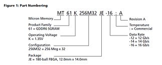
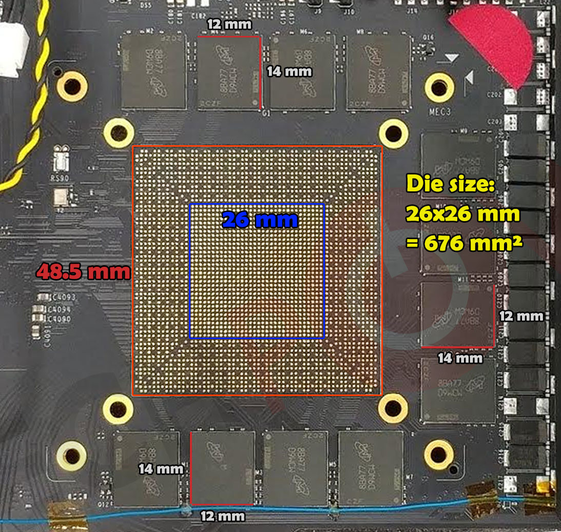
Update:
I tried to estimate die size from the photo. We do know from the datasheet that the GDDR6 memory chips are 14 mm x 12 mm. Based on that information I rescaled, warped and straightened the image, so that each GDDR6 memory chip is 140 x 120 pixels. With all memory chips around the GPU now being at the correct size, we can use the GPU's silkscreen print to estimate the actual size of the chip package, which I measured at 48.5 x 48.5 mm. Assuming that the inner silk screen with the solder balls represents the surface of the GPU die, we get a length of 26 mm for each side of the die, which brings die size to 676 mm². This makes it a relatively large die considering NVIDIA's existing lineup: GV100 (815 mm², Titan V), GP100 (610 mm², Quadro GP100), GP102 (471 mm², GTX 1080 Ti), GP104 (314 mm², GTX 1080), GP106 (200 mm², GTX 1060). So my initial assessment that this could be the GP102 successor seems accurate, especially since GV100 die size is quite a bit bigger than GP100 die size, by roughly 33%. Our calculated GV102 die size is 40% bigger than GP102, which falls in that range.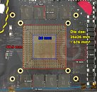
Source:
Reddit
The card is clearly made by NVIDIA as indicated by the markings near the PCI-Express x16 slot connector. What's also visible is three PCI-Express 8-pin power inputs and a huge VRM setup with four fans. Unfortunately the GPU in the center of the board is missing, but it should be GV102, the successor to GP102, since GDDR6 support is needed. The twelve GDDR6 memory chips located around the GPU's solder balls are marked as D9WCW, which decodes to MT61K256M32JE-14:A. These chips are Micron-made 8 Gbit GDDR6, specified for 14 Gb/s data rate, operating at 1.35 V. With twelve chips, this board has a 384-bit memory bus and 12 GB VRAM. The memory bandwidth at 14 Gbps data rate is a staggering 672 GB/s, which conclusively beats the 484 GB/s that Vega 64 and GTX 1080 Ti offer.
My take on this whole board, mostly due to the overkill power supply (up to 525 W) and the amount of test points and jumpers is that this board is used to test and qualify performance and power consumption in an unconstrained way, so that engineers and marketing can later decide on acceptable power and performance targets for release. The NVLink connector and functionality can also be tested at this stage, and the final PCB for mass production will be designed based on the outcome of these tests. On the bottom left of the PCB we find a mini-DP connector, which should be perfectly sufficient for this kind of testing, but not for a retail board.
Near the far right of the photo, rotated by 90 degrees, we see some mechanical drawings that to me, look like a new retention plate for the cooler. You can clearly see some space inside, which seems to be for the graphics processor itself. Around that are some mounting holes, which look like they are for a cooling solution.

I tried to estimate die size from the photo. We do know from the datasheet that the GDDR6 memory chips are 14 mm x 12 mm. Based on that information I rescaled, warped and straightened the image, so that each GDDR6 memory chip is 140 x 120 pixels. With all memory chips around the GPU now being at the correct size, we can use the GPU's silkscreen print to estimate the actual size of the chip package, which I measured at 48.5 x 48.5 mm. Assuming that the inner silk screen with the solder balls represents the surface of the GPU die, we get a length of 26 mm for each side of the die, which brings die size to 676 mm². This makes it a relatively large die considering NVIDIA's existing lineup: GV100 (815 mm², Titan V), GP100 (610 mm², Quadro GP100), GP102 (471 mm², GTX 1080 Ti), GP104 (314 mm², GTX 1080), GP106 (200 mm², GTX 1060). So my initial assessment that this could be the GP102 successor seems accurate, especially since GV100 die size is quite a bit bigger than GP100 die size, by roughly 33%. Our calculated GV102 die size is 40% bigger than GP102, which falls in that range.
77 Comments on NVIDIA GV102 Prototype Board With GDDR6 Spotted, Up to 525 W Power Delivery. GTX 1180 Ti?
610 gp100
470 gp102 same core count
So 800 to 600 is plausable 5120 each
GV104 will have 4 GPCs, 56 SMs, and 3584 Cuda cores.
GV106 will have 2 GPCs, 28 SMs, and 1792 Cuda cores.
GV102 will have fewer fp64 units, but we don't yet know if the tensor unit count is the same.
TSMCs 12nm process offers about 20% higher density.. They would have to go beyond 400mm² for 40% cores, something they haven't done for their high end chips.
Where do you get that TSMC's "12 nm" is 20% denser? GV100 is not denser, and TSMC "12 nm" is still the same node just with improved thermals. Pascal is not pushing the maximum density of TSMC's "16 nm". Expect the density of GV102/GV104 to be in the same range as before.
Removed tensor cores and theres your space
We don't even know yet if "GV104" and "GV102" will be segmented the same way as GP104 and GP102. Titan and Quadro are already using the GV100 die, so it will be interesting if Nvidia carve out more than one bin of "GV102", and if multiple of those will be consumer products.
GV100 non-gl
Heres 15 pages of SLI supported games.. www.geforce.com/hardware/technology/sli/games
The right card is a 150w full Volta core enabled Tesla... albeit greatly reduced clocks. SXM2 is 300w, full sized pcie 250w, and baby volta 150w.
The SXM2 cards are pretty nuts...
Had to go dig through my pictures, the baby v100 (150w variant) is not nvlink enabled, no gold finger, the big one can do 2 way, and the sxm2 can do 4/8/16 way. Most servers are 4 or 8 sxm2 though... only dgx2 supports 16 way...and costs what 400k.
My guess would be quadro or consumer volta/turning sample for testing gddr6.