Apr 1st, 2025 14:25 EDT
change timezone
Latest GPU Drivers
New Forum Posts
- Is the futureproof gaming solution a four drive system? (30)
- RX 9070 availability (253)
- What's your latest tech purchase? (23441)
- lowering the voltage but performance decreased a lot. (1)
- Rtx 3060 laptop no longer working after wrong vbios flash (19)
- Opened Thaiphoon then crash! (1)
- WCG Daily Numbers (12823)
- Can you guess Which game it is? (53)
- AIO - 120mm cpu cooler? (42)
- Msi Vector 16HX Undervolt (9)
Popular Reviews
- DDR5 CUDIMM Explained & Benched - The New Memory Standard
- Sapphire Radeon RX 9070 XT Pulse Review
- ASRock Phantom Gaming B850 Riptide Wi-Fi Review - Amazing Price/Performance
- SilverStone Lucid 04 Review
- Palit GeForce RTX 5070 GamingPro OC Review
- Samsung 9100 Pro 2 TB Review - The Best Gen 5 SSD
- Sapphire Radeon RX 9070 XT Nitro+ Review - Beating NVIDIA
- Enermax REVOLUTION D.F. 12 850 W Review
- Assassin's Creed Shadows Performance Benchmark Review - 30 GPUs Compared
- AMD Ryzen 7 9800X3D Review - The Best Gaming Processor
Controversial News Posts
- MSI Doesn't Plan Radeon RX 9000 Series GPUs, Skips AMD RDNA 4 Generation Entirely (144)
- Microsoft Introduces Copilot for Gaming (124)
- AMD Radeon RX 9070 XT Reportedly Outperforms RTX 5080 Through Undervolting (119)
- NVIDIA Reportedly Prepares GeForce RTX 5060 and RTX 5060 Ti Unveil Tomorrow (115)
- Over 200,000 Sold Radeon RX 9070 and RX 9070 XT GPUs? AMD Says No Number was Given (100)
- NVIDIA GeForce RTX 5050, RTX 5060, and RTX 5060 Ti Specifications Leak (96)
- Retailers Anticipate Increased Radeon RX 9070 Series Prices, After Initial Shipments of "MSRP" Models (90)
- China Develops Domestic EUV Tool, ASML Monopoly in Trouble (88)
Tuesday, June 26th 2018

NVIDIA GV102 Prototype Board With GDDR6 Spotted, Up to 525 W Power Delivery. GTX 1180 Ti?
Reddit user 'dustinbrooks' has posted a photo of a prototype graphics card design that is clearly made by NVIDIA and "tested by a buddy of his that works for a company that tests NVIDIA boards". Dustin asked the community what he was looking at, which of course got tech enthusiasts interested.
The card is clearly made by NVIDIA as indicated by the markings near the PCI-Express x16 slot connector. What's also visible is three PCI-Express 8-pin power inputs and a huge VRM setup with four fans. Unfortunately the GPU in the center of the board is missing, but it should be GV102, the successor to GP102, since GDDR6 support is needed. The twelve GDDR6 memory chips located around the GPU's solder balls are marked as D9WCW, which decodes to MT61K256M32JE-14:A. These chips are Micron-made 8 Gbit GDDR6, specified for 14 Gb/s data rate, operating at 1.35 V. With twelve chips, this board has a 384-bit memory bus and 12 GB VRAM. The memory bandwidth at 14 Gbps data rate is a staggering 672 GB/s, which conclusively beats the 484 GB/s that Vega 64 and GTX 1080 Ti offer.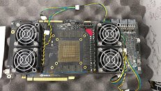 Looking to the top edge of the PCB we see a connector similar to NVIDIA's NVLink connector, but it's missing half of its pins, which means daisy chaining more than two cards won't be possible. Maybe NVIDIA plans to segment NVLink to "up to two" and "more than two", with the latter of course being much more pricey, similar to how server processors are segmented by their multi-processor support. It could also be a new kind of SLI connector, which I'm not sure about, as GPU vendors want to get rid of this multi-GPU approach.
My take on this whole board, mostly due to the overkill power supply (up to 525 W) and the amount of test points and jumpers is that this board is used to test and qualify performance and power consumption in an unconstrained way, so that engineers and marketing can later decide on acceptable power and performance targets for release. The NVLink connector and functionality can also be tested at this stage, and the final PCB for mass production will be designed based on the outcome of these tests. On the bottom left of the PCB we find a mini-DP connector, which should be perfectly sufficient for this kind of testing, but not for a retail board.
Near the far right of the photo, rotated by 90 degrees, we see some mechanical drawings that to me, look like a new retention plate for the cooler. You can clearly see some space inside, which seems to be for the graphics processor itself. Around that are some mounting holes, which look like they are for a cooling solution.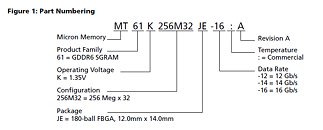
Update:
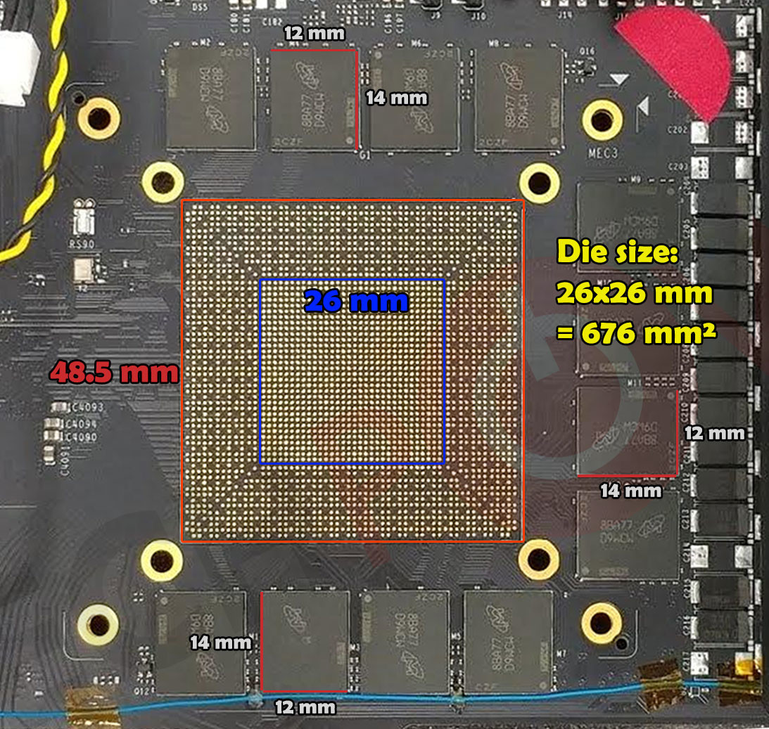
I tried to estimate die size from the photo. We do know from the datasheet that the GDDR6 memory chips are 14 mm x 12 mm. Based on that information I rescaled, warped and straightened the image, so that each GDDR6 memory chip is 140 x 120 pixels. With all memory chips around the GPU now being at the correct size, we can use the GPU's silkscreen print to estimate the actual size of the chip package, which I measured at 48.5 x 48.5 mm. Assuming that the inner silk screen with the solder balls represents the surface of the GPU die, we get a length of 26 mm for each side of the die, which brings die size to 676 mm². This makes it a relatively large die considering NVIDIA's existing lineup: GV100 (815 mm², Titan V), GP100 (610 mm², Quadro GP100), GP102 (471 mm², GTX 1080 Ti), GP104 (314 mm², GTX 1080), GP106 (200 mm², GTX 1060). So my initial assessment that this could be the GP102 successor seems accurate, especially since GV100 die size is quite a bit bigger than GP100 die size, by roughly 33%. Our calculated GV102 die size is 40% bigger than GP102, which falls in that range.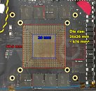
Source:
Reddit
The card is clearly made by NVIDIA as indicated by the markings near the PCI-Express x16 slot connector. What's also visible is three PCI-Express 8-pin power inputs and a huge VRM setup with four fans. Unfortunately the GPU in the center of the board is missing, but it should be GV102, the successor to GP102, since GDDR6 support is needed. The twelve GDDR6 memory chips located around the GPU's solder balls are marked as D9WCW, which decodes to MT61K256M32JE-14:A. These chips are Micron-made 8 Gbit GDDR6, specified for 14 Gb/s data rate, operating at 1.35 V. With twelve chips, this board has a 384-bit memory bus and 12 GB VRAM. The memory bandwidth at 14 Gbps data rate is a staggering 672 GB/s, which conclusively beats the 484 GB/s that Vega 64 and GTX 1080 Ti offer.
My take on this whole board, mostly due to the overkill power supply (up to 525 W) and the amount of test points and jumpers is that this board is used to test and qualify performance and power consumption in an unconstrained way, so that engineers and marketing can later decide on acceptable power and performance targets for release. The NVLink connector and functionality can also be tested at this stage, and the final PCB for mass production will be designed based on the outcome of these tests. On the bottom left of the PCB we find a mini-DP connector, which should be perfectly sufficient for this kind of testing, but not for a retail board.
Near the far right of the photo, rotated by 90 degrees, we see some mechanical drawings that to me, look like a new retention plate for the cooler. You can clearly see some space inside, which seems to be for the graphics processor itself. Around that are some mounting holes, which look like they are for a cooling solution.

I tried to estimate die size from the photo. We do know from the datasheet that the GDDR6 memory chips are 14 mm x 12 mm. Based on that information I rescaled, warped and straightened the image, so that each GDDR6 memory chip is 140 x 120 pixels. With all memory chips around the GPU now being at the correct size, we can use the GPU's silkscreen print to estimate the actual size of the chip package, which I measured at 48.5 x 48.5 mm. Assuming that the inner silk screen with the solder balls represents the surface of the GPU die, we get a length of 26 mm for each side of the die, which brings die size to 676 mm². This makes it a relatively large die considering NVIDIA's existing lineup: GV100 (815 mm², Titan V), GP100 (610 mm², Quadro GP100), GP102 (471 mm², GTX 1080 Ti), GP104 (314 mm², GTX 1080), GP106 (200 mm², GTX 1060). So my initial assessment that this could be the GP102 successor seems accurate, especially since GV100 die size is quite a bit bigger than GP100 die size, by roughly 33%. Our calculated GV102 die size is 40% bigger than GP102, which falls in that range.
Apr 1st, 2025 14:25 EDT
change timezone
Latest GPU Drivers
New Forum Posts
- Is the futureproof gaming solution a four drive system? (30)
- RX 9070 availability (253)
- What's your latest tech purchase? (23441)
- lowering the voltage but performance decreased a lot. (1)
- Rtx 3060 laptop no longer working after wrong vbios flash (19)
- Opened Thaiphoon then crash! (1)
- WCG Daily Numbers (12823)
- Can you guess Which game it is? (53)
- AIO - 120mm cpu cooler? (42)
- Msi Vector 16HX Undervolt (9)
Popular Reviews
- DDR5 CUDIMM Explained & Benched - The New Memory Standard
- Sapphire Radeon RX 9070 XT Pulse Review
- ASRock Phantom Gaming B850 Riptide Wi-Fi Review - Amazing Price/Performance
- SilverStone Lucid 04 Review
- Palit GeForce RTX 5070 GamingPro OC Review
- Samsung 9100 Pro 2 TB Review - The Best Gen 5 SSD
- Sapphire Radeon RX 9070 XT Nitro+ Review - Beating NVIDIA
- Enermax REVOLUTION D.F. 12 850 W Review
- Assassin's Creed Shadows Performance Benchmark Review - 30 GPUs Compared
- AMD Ryzen 7 9800X3D Review - The Best Gaming Processor
Controversial News Posts
- MSI Doesn't Plan Radeon RX 9000 Series GPUs, Skips AMD RDNA 4 Generation Entirely (144)
- Microsoft Introduces Copilot for Gaming (124)
- AMD Radeon RX 9070 XT Reportedly Outperforms RTX 5080 Through Undervolting (119)
- NVIDIA Reportedly Prepares GeForce RTX 5060 and RTX 5060 Ti Unveil Tomorrow (115)
- Over 200,000 Sold Radeon RX 9070 and RX 9070 XT GPUs? AMD Says No Number was Given (100)
- NVIDIA GeForce RTX 5050, RTX 5060, and RTX 5060 Ti Specifications Leak (96)
- Retailers Anticipate Increased Radeon RX 9070 Series Prices, After Initial Shipments of "MSRP" Models (90)
- China Develops Domestic EUV Tool, ASML Monopoly in Trouble (88)
77 Comments on NVIDIA GV102 Prototype Board With GDDR6 Spotted, Up to 525 W Power Delivery. GTX 1180 Ti?
I mean, can you name any other technology that became a success after failing to break 2% market penetration 10+ years after its commercial release?
Unless there is more memory chips on the other side of the PCB, which seems unlikely.
With the 10xx series, nvida made it harder. For reasons never explained, SLI average scaling at 1080p was only 18% ... @ 1440p, about 30%. Yet for some reason, at 2160p it was well over 55% with some games scaling near 100%. Looking at the numbers, it does seem off that the proce equartion was no longer valid at 1080p and 1440p where the top tier card was now keeping ya well above 60 fps. But where it couldn't, SLI managed to make sense at 2160p. With thr 4k HDR panels about to drop at $1,999 or so... they will be too high priced for mainstream users and i don't see a chnage in the parigm until these things drop into the range of affordability. But as monitor technology improvements continue to bring us more pixels, I don't see nVidia abandoning a multi GPU option at the high end.
SLI has never worked as well as you described. And Nvidia have not deliberately sabotaged their Pascal cards, but SLI support in top games have decreased over the last years, due to most top games being console ports. SLI support is highly dependent on how the game engine works, and Nvidia with all their driver tricks can't make a game which is not suited scale with SLI. Current games commonly use multi-pass rendering with synchronization and post-processing effects which limits multi-GPU scaling.
SLI has never been a good choice to get "cheap high-end performance"; SLI has only worked well in certain games, full of glitches and riddled with stutter. SLI is and have just been an option for those who "need" more performance than a single card can offer, in select titles.
and i mean massive TDP like vega56/64 and 64 watercool way. loosers choice amd.
vega64 power eat juice is close that 500W with oc's and its so high that that amd gpu should just banned and get penalty ticket for amd.
nvidia politics are faraway thouse 'we dont care' politics.
300W is limit for nvidia,and that only special gpus like titan.
turing 1060 beat vega 64.