Saturday, November 17th 2018

Samsung AMD's Second Foundry Partner for "Polaris 30"
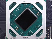
AMD's "Polaris 30" silicon at the heart of Radeon RX 590 graphics card is the company's first 12 nm GPU. Unlike NVIDIA, which is exclusively sourcing its "Turing" family of GPUs from TSMC, the "Polaris 30" is coming from not one, but two sources. This, according to AMD in response to a question by TechPowerUp. The two foundries manufacturing "Polaris 30" are GlobalFoundries and Samsung. AMD did not provide us with visual cues on how to tell chips made from either foundries apart (such as serial numbering schemes). Packaging of dies sourced from both foundries is done in China, and the national-origin marking for the chip is on the package, rather than printed on the die.
GlobalFoundries' 12 nanometer FinFET node, called GloFo 12LP, shares a lot of similarities with Samsung's 11LPP, because both are "nodelets" that are derived from an original 14 nm FinFET process blueprint Samsung licensed to GloFo, deployed in its facility in upstate New York, where AMD's "Zen" processors are made. GloFo's 12 nanometer process is a refinement of its 14 nm node, in which 12 nm transistors are etched onto silicon using the same lithography meant for 14 nm. It doesn't improve transistor densities, but provides dividends in power, which explains why "Polaris 30" and "Pinnacle Ridge" have the same die sizes as "Polaris 20" and "Summit Ridge," respectively. This WikiChip article provides a good explanation of how GloFo 12LP is a nodelet.AMD appears highly motivated to be first-to-market with both 7 nm CPU and GPU, which come in the form of its "Vega 20" GPU and "Rome" CPU, which could be formally launched before the end of 2018, with production being ramped up through 2019. AMD confirmed publicly earlier, that its first 7 nm chips could be sourced from TSMC, but even it realizes that TSMC has an exhaustive list of clientele for 7 nm, each with its own foundry allocation. AMD could try to find additional sources for 7 nm chips, and we predict Samsung to be one of them. GloFo canned its 7 nm plans, and AMD is keeping it busy with wafer contracts for "Zen," "Zen+," "Polaris," "Vega 10" GPU die, and the 14 nm I/O controller die at the heart of its EPYC "Rome" MCM.
GlobalFoundries' 12 nanometer FinFET node, called GloFo 12LP, shares a lot of similarities with Samsung's 11LPP, because both are "nodelets" that are derived from an original 14 nm FinFET process blueprint Samsung licensed to GloFo, deployed in its facility in upstate New York, where AMD's "Zen" processors are made. GloFo's 12 nanometer process is a refinement of its 14 nm node, in which 12 nm transistors are etched onto silicon using the same lithography meant for 14 nm. It doesn't improve transistor densities, but provides dividends in power, which explains why "Polaris 30" and "Pinnacle Ridge" have the same die sizes as "Polaris 20" and "Summit Ridge," respectively. This WikiChip article provides a good explanation of how GloFo 12LP is a nodelet.AMD appears highly motivated to be first-to-market with both 7 nm CPU and GPU, which come in the form of its "Vega 20" GPU and "Rome" CPU, which could be formally launched before the end of 2018, with production being ramped up through 2019. AMD confirmed publicly earlier, that its first 7 nm chips could be sourced from TSMC, but even it realizes that TSMC has an exhaustive list of clientele for 7 nm, each with its own foundry allocation. AMD could try to find additional sources for 7 nm chips, and we predict Samsung to be one of them. GloFo canned its 7 nm plans, and AMD is keeping it busy with wafer contracts for "Zen," "Zen+," "Polaris," "Vega 10" GPU die, and the 14 nm I/O controller die at the heart of its EPYC "Rome" MCM.

41 Comments on Samsung AMD's Second Foundry Partner for "Polaris 30"
They will all get euv lines within the same few years but they still wont quite be used the same yet net result is the same, what they say is a 7nm chip.
Even Intel's attempts to make every fab identical do not result in identical production runs, far from it even. Look at the 8700K.
Sound logic no?