News Posts matching #Zen+

Return to Keyword Browsing

AMD Patches Zenbleed Vulnerability with AGESA 1.2.0.Ca Update

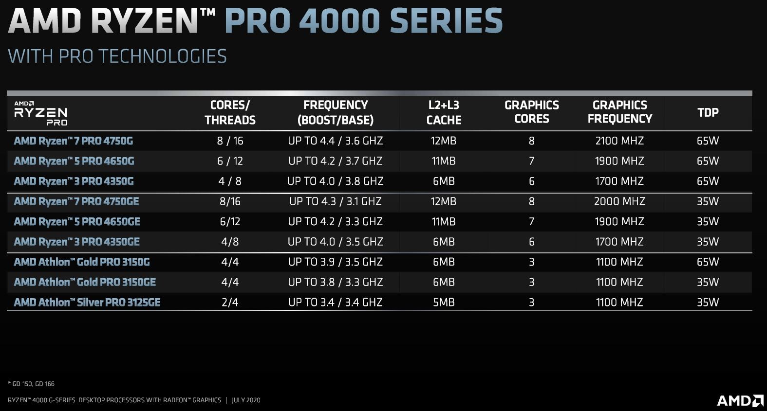
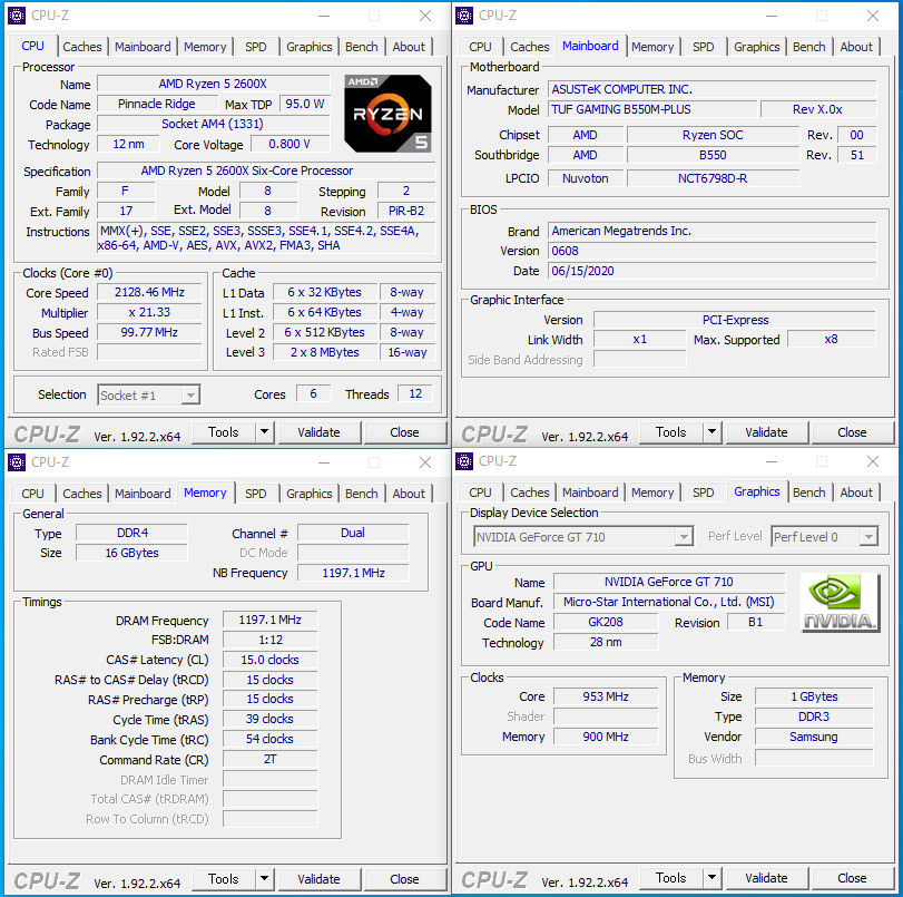
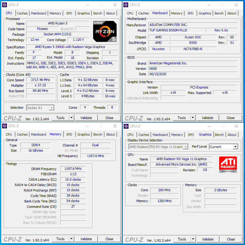
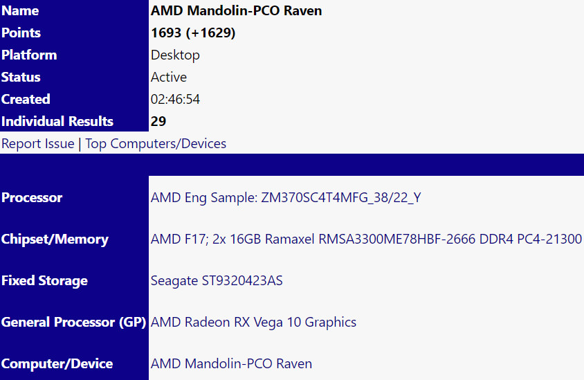
AMD classified the Zenbleed vulnerability, CVE-2023-20593, as a medium-level threat about a year ago. AMD has acknowledged that it could potentially allow an attacker to access sensitive information under certain microarchitectural circumstances. Today, MSI has released new BIOS updates featuring AMD's AM4 AGESA 1.2.0.Ca firmware update. This update addresses the Zenbleed vulnerability affecting AMD's Ryzen 4000 series Zen 2 APUs. MSI is proactively rolling out the new BIOS updates across its range of compatible motherboards. The updates are currently available for almost all X570 motherboards, with support for other chipsets and 400 series motherboards expected to follow soon.

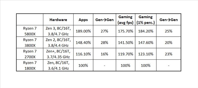
The AGESA 1.2.0.Ca firmware update specifically targets the Zenbleed vulnerability in the Zen 2 microarchitecture. Although the vulnerability primarily affects Ryzen 4000 "Renoir" APUs, it also exists in other Zen 2 processors, including the Ryzen 3000 series and certain EPYC and Threadripper CPUs. AMD has already addressed the Zenbleed vulnerability in previous AGESA microcode updates for Ryzen 3000 processors and other platforms, such as EPYC server CPUs and Ryzen mobile CPUs. However, the Ryzen Embedded V2000 CPUs are still awaiting the EmbeddedPi-FP6 1.0.0.9 AGESA firmware update, which is expected to be released by April. While AMD has not explicitly stated whether the security update will impact performance, previous testing of Zenbleed fixes has shown potential performance drops of up to 15% in certain workloads, although gaming performance remained relatively unaffected. Users with AM4 chips based on architectures other than Zen 2, such as Zen+ or Zen 3, do not need to update their BIOS as they are not affected by this specific vulnerability.

AMD Confirms Optical-Shrink of Zen 4 to the 4nm Node in its Latest Roadmap

AMD in its Ryzen 7000 series launch event shared its near-future CPU architecture roadmap, in which it confirmed that the "Zen 4" microarchitecture, currently on the 5 nm foundry node, will see an optical-shrink to the 4 nm process in the near future. This doesn't necessarily indicate a new-generation CCD (CPU complex die) on 4 nm, it could even be a monolithic mobile SoC on 4 nm, or perhaps even "Zen 4c" (high core-count, low clock-speed, for cloud-compute); but it doesn't rule out the possibility of a 4 nm CCD that the company can use across both its enterprise and client processors.

The last time AMD hyphenated two foundry nodes for a single generation of the "Zen" architecture, was with the original (first-generation) "Zen," which debuted on the 14 nm node, but was optically shrunk and refined on the 12 nm node, with the company designating the evolution as "Zen+." The Ryzen 7000-series desktop processors, as well as the upcoming EPYC "Genoa" server processors, will ship with 5 nm CCDs, with AMD ticking it off in its roadmap. Chronologically placed next to it are "Zen 4" with 3D Vertical Cache (3DV Cache), and the "Zen 4c." The company is planning "Zen 4" with 3DV Cache both for its server- and desktop segments. Further down the roadmap, as we approach 2024, we see the company debut the future "Zen 5" architecture on the same 4 nm node, evolving into 3 nm on certain variants.

AMD Confirms "Zen 3" with 64 MB 3DV Cache for Q1-2022, "Zen 4" Later, PCIe Gen5 + DDR5

AMD today celebrated 5 Years of Ryzen, with a special video presentation by John Taylor, AMD Chief Marketing Officer, and Robert Hallock, Director of Technical Marketing. The company confirmed that its next Ryzen processors will come out only in Q1-2022. These processors will feature updated CPU core complex dies (CCDs) that combine the existing "Zen 3" microarchitecture with 64 MB of additional 3D Vertical Cache memory. AMD claims that this change improves performance by anywhere between 4% to 25% for games, amounting to the kind of performance uplifts you'd expect from a new processor generation.

AMD did not reveal whether the updated processors will be branded within the existing Ryzen 5000 series, or newer Ryzen 6000 series. If you remember, the "Zen+" microarchitecture enabled AMD to come up with a whole new generation, the Ryzen 2000 series, despite modest 4% IPC uplifts, albeit significant improvements to the boosting behavior, resulting in improved multi-threaded performance. What remains unclear is whether the updated "Zen 3" chips with 3DV Cache will herald a new platform, or whether these chips will be built on the existing Socket AM4 with DDR4 memory and PCI-Express Gen 4.

Intel Core i9-12900K "Alder Lake" Beats Ryzen Threadripper 2990WX at Cinebench R23 nT

An alleged Intel Core i9-12900K "Alder Lake-S" sample is shown beating the 32-core AMD Ryzen Threadripper 2990WX HEDT processor at AMD's favorite benchmark, Cinebench R23, in its multi-threaded (nT) test. At this point it's not known whether the i9-12900K is overclocked, but the CPU-Z instance in the screenshot reads 5.30 GHz, which could very well be the processor's stock Thermal Velocity Boost frequency. The sample scored upward of 30000 points, putting it above the Threadripper 2990WX reference score in Cinebench.

The 2990WX is based on the "Zen+" microarchitecture, and released in 2018, but is a 32-core/64-thread chip that should have ripped through this rendering workload. The i9-12900K, on the other hand, has eight "Golden Cove" performance cores that have HyperThreading, in addition to 8 "Gracemont" efficiency cores that lack HTT. This benchmark was run on Windows 10, which lacks awareness of the Intel Thread Director, a hardware component that optimizes utilization of the two kinds of CPU cores. Windows 11 is known to feature better awareness of hybrid core architectures. The i9-12900K sample is possibly installed on a Gigabyte Z690 AORUS Ultra motherboard, and has 32 GB of DDR5-5200 memory (two modules, logically four 40-bit channels).

Meltdown-like Vulnerability Affects AMD Zen+ and Zen2 Processors

Cybersecurity researchers Saidgani Musaev and Christof Fetzer with the Dresden Technology University discovered a novel method of forcing illegal data-flow between microarchitectural elements on AMD processors based on the "Zen+" and "Zen 2" microarchitectures, titled "Transient Execution of Non-canonical Accesses." The method was discovered in October 2020, but the researchers followed responsible-disclosure norms, giving AMD time to address the vulnerability and develop a mitigation. The vulnerability is chronicled under CVE-2020-12965 and AMD Security Bulletin ID "AMD-SB-1010."

The one-line summary of this vulnerability from AMD reads: "When combined with specific software sequences, AMD CPUs may transiently execute non-canonical loads and store using only the lower 48 address bits, potentially resulting in data leakage." The researchers studied this vulnerability on three processors, namely the EPYC 7262 based on "Zen 2," and Ryzen 7 2700X and Ryzen Threadripper 2990WX, based on "Zen+." They mention that all Intel processors that are vulnerable to MDS attacks "inherently have the same flaw." AMD is the subject of the paper as AMD "Zen+" (and later) processors are immune to MDS as demonstrated on Intel processors. AMD developed a mitigation for the vulnerability, which includes ways of patching vulnerable software.

Find the security research paper here (PDF), and the AMD security bulletin here. AMD's mitigation blueprint can be accessed here.

The Ultimate Zen: AMD's Zen 3 Achieves 89% Higher Performance Than First-generation Zen

An investigative, generation-upon-generation review from golem.de paints an extremely impressive picture for AMD's efforts in iterating upon their original Zen architecture. While the first generation Zen achieved a sorely needed inflection point in the red team's efforts against arch-rival Intel and its stranglehold in the high-performance CPU market, AMD couldn't lose its vision on generational performance improvements on pain of being steamrolled (pun intended) by the blue giant's sheer scale and engineering prowess. However, perhaps this is one of those showcases of "small is nimble", and we're now watching Intel slowly changing its posture, crushed under its own weight, so as to offer actual competition to AMD's latest iteration of the Zen microarchitecture.

The golem.de review compares AMD's Zen, Zen+, Zen 2 and Zen 3 architectures, represented by the Ryzen 7 1800X, Ryzen 7 2700X, Ryzen 7 3800X and Ryzen 7 5800X CPUs. Through it, we see a generational performance increase that mostly exceeds the 20% performance points across every iteration of Zen when it comes to both gaming and general computing workloads. This generational improvement hits its (nowadays) most expressive result in that AMD's Ryzen 7 5800X manages to deliver 89% higher general computing, and 84% higher gaming performance than the company's Zen-based Ryzen 7 1800X. And this, of course, ignoring performance/watt improvements that turn the blue giant green with envy.

AMD Ryzen 3000C-series Processors Based on Existing "Zen+" IP, Heavy TDP Optimization

AMD earlier today announced its Ryzen 3000C-series processors targeted at Chromebooks, a segment where the company feels it can bring more to the table than Intel's entry-level Celeron, Pentium Silver, and Pentium Gold mobile processors. Responding to a questionnaire by TechPowerUp, AMD revealed a handful details about these processors. The Ryzen 3000C-series processors are based on the 12 nm "Picasso" silicon, while the Athlon Gold and Athlon Silver parts are based on 14 nm. The "Picasso" based parts combine up to 4 "Zen+" CPU cores, with an iGPU based on the "Vega" graphics architecture, with up to 10 NGCUs. AMD has optimized all SKUs for a 15 W TDP target.

Responding to a question on storage specification or possible collaboration with MediaTek on WLAN controllers, AMD responded that it wishes a diverse hardware ecosystem for its OEM partners, without getting into specifics. There was no denial on the MediaTek bit. The Ryzen 7 3700C practically maxes out the "Picasso" silicon within the 15 W TDP envelope, which got us wondering if AMD has its eyes on the premium Chromebook segment, possibly even Google's first-party Chromebook Pixel brand. To this company responded that while the 3700C has a solid feature-set for premium Chromebooks, there are no first-party Pixel products on the anvil. AMD has just entered the market, and possibly wants to make a dent on the bulk of the Chromebook market first.

AMD Announces Renoir for Desktop: Ryzen 4000G, PRO 4000G, and Athlon PRO 3000G

AMD today announced its 4th Generation Ryzen 4000G and Ryzen PRO 4000G desktop processors for pre-built OEM desktops. The company also expanded its entry-level Athlon 3000G series and debuted the Athlon PRO 3000G series. The Ryzen 4000G and PRO 4000G mark the Socket AM4 desktop debut of the 7 nm "Renoir" silicon, which combines up to 8 CPU cores based on the "Zen 2" microarchitecture, with a Radeon Vega 8 iGPU. These processors benefit from the 65 W TDP and increased power limits of the desktop platform to dial up CPU- and iGPU engine clock speeds significantly over the Ryzen 4000U and 4000H mobile processors based on the same silicon. The new Athlon 3000G-series and Athlon PRO 3000G-series parts are based on a 12 nm die that has "Zen+" CPU cores.

All of the processor models announced today are OEM-only, meaning that you'll only find them on pre-built consumer- and commercial desktops by the likes of HP, Lenovo, Dell, etc. Not even the system-integrator (SI) channel (eg: Maingear, Origin PC, etc.,) gets these chips. OEMs will pair these processors with motherboards based on the AMD B550 chipset, although the chips are compatible with the X570 chipset, too. The Ryzen PRO 4000G processors are targeted at commercial desktops that are part of large business environments, and launches along with the new AMD PRO565 chipset. Since they are OEM-only, the company did not reveal pricing for any of these chips. They did however mention that for the DIY retail channel, they do plan to update their product stack with processors that have integrated graphics at a later time (without going into specifics of the said time).

AMD B550 Motherboard Shown Running Zen+ "Pinnacle Ridge" and "Picasso" CPUs

The AMD B550 chipset isn't supposed to run 1st- and 2nd-generation AMD Ryzen processors, or even Ryzen 5 3400G and 3200G APUs based on the older "Zen+" microarchitecture. AMD specifically made a packaging badge that reflects this. The B550 chipset only supports 3rd gen Ryzen "Matisse," and is ready for upcoming "Renoir" and "Zen 3" based "Vermeer" processors, when they do come out.

Given this, imagine our surprise when someone with access to a B550 motherboard was able to run older processors on it. PC enthusiast 188 "momomo_us" posted screenshots of an ASUS TUF Gaming B550M-Plus motherboard running "Zen+" based Ryzen 5 3400G APU based on the "Picasso" silicon, and Ryzen 5 2600X processor based on the "Pinnacle Ridge" silicon, complete with CPU-Z validations. The board is shown running BIOS version 0608 (dated 15/06/2020). There's nothing in the official change-log to indicate Zen+ support, nor in its CPU support list, and the CPU-Z screenshots don't reveal AGESA version in the BIOS version string. An impressive feat nonetheless. We still can't recommend taking the risk of buying B550 motherboards with older processors. Find the CPU-Z validation for the 3400G+B550 and 2600X+B550.

AMD Updates Ryzen 3 1200 CPU with Zen+ Architecture

AMD has reportedly updated its Ryzen 3 1200 CPU with Zen+ architecture and is now offering it to consumers. Featuring a configuration of 4 cores with 4 threads, this CPU can operate anywhere from 3.1 GHz (base) to 3.4 GHz in boost frequency. Having originally launched in July of 2017, just under three years ago, AMD decided to refresh this CPU with Zen+ architecture, which brought improvements like a tiny IPC increase, better turbo boost speeds, faster caches and better memory controller for better support of faster DDR4 modules.

The new "Zen+" revision has the same specifications as the older model, however, the only difference is the newer 12 nm manufacturing process and some of the architecture changes of Zen+. The rest of the specifications like clock speeds are the same. The CPU is listed by a German supplier for €54.73 or about $60. This revision carries a different part number, under the code "YD1200BBM4KAFBOX", where the older 14 nm model was "YD1200BBM4KAEBOX".
AMD Ryzen 3 1200 12nm Zen+ Edition

AMD Processors Since 2011 Hit with Cache Attack Vulnerabilities: Take A Way

Cybersecurity researcher Moritz Lipp and his colleagues from the Graz University of Technology and the University of Rennes uncovered two new security vulnerabilities affecting all AMD CPU microarchitectures going back to 2011, detailed in a research paper titled "Take A Way." These include "Bulldozer" and its derivatives ("Piledriver," "Excavator," etc.,) and the newer "Zen," "Zen+," and "Zen 2" microarchitectures. The vulnerabilities are specific to AMD's proprietary L1D cache way predictor component. It is described in the security paper's abstract as a means for the processor to "predict in which cache way a certain address is located, so that consequently only that way is accessed, reducing the processor's power consumption."

By reverse engineering the L1D cache way predictor in AMD microarchitectures dating from 2011 to 2019, Lipp, et al, discovered two new attack vectors with which an attacker can monitor the victim's memory accesses. These vectors are named "Collide+Probe," and "Load+Reload." The paper describes the first vector as follows: "With Collide+Probe, an attacker can monitor a victim's memory accesses without knowledge of physical addresses or shared memory when time-sharing a logical core." The second vector is described as "With Load+Reload, we exploit the way predictor to obtain highly-accurate memory-access traces of victims on the same physical core." The two vulnerabilities have not been assigned CVE entries at the time of this writing. The research paper, however, describes the L1D cache way predictor in AMD processors as being vulnerable to attacks that can reveal contents of memory or even keys to a vulnerable AES implementation. For now there is no mitigation to these attacks, but the company is reportedly working on firmware and driver updates. Access the research paper here.
AMD L1D cache way predictor logic found vulnerable in Take A Way attack classes.

AMD Announces Ryzen 9 3950X, Details 3rd Gen Ryzen Threadripper, unlocked Athlon 3000G

AMD today announced four new desktop processors across three very diverse markets. To begin with, the company crowned its socket AM4 mainstream desktop platform with the mighty new Ryzen 9 3950X processor. Next up, it released its new baseline entry-level APU, the Athlon 3000G. Lastly, it detailed the 3rd generation Ryzen Threadripper HEDT processor family with two initial models, the Ryzen Threadripper 3960X and the flagship Ryzen Threadripper 3970X. The company also formally released its AGESA Combo PI 1.0.0.4B microcode, and with it, introduced a killer new feature for all "Zen 2" based Ryzen processors, called ECO Mode.

The Ryzen 9 3950X is a 16-core/32-thread processor in the AM4 package, compatible with all socket AM4 motherboards, provided they have the latest BIOS update with AGESA Combo PI 1.0.0.4B microcode. The processor comes with clock-speeds of 3.50 GHz base, with 4.70 GHz maximum boost frequency, and the same 105 W TDP as the 12-core Ryzen 9 3900X. With 512 KB of dedicated L2 cache per core, and 64 MB of shared L3 cache, the chip has a mammoth 72 MB of "total cache."

AMD Designing Zen 4 for 2021, Zen 3 Completes Design Phase, out in 2020

AMD in its 2nd generation EPYC processor launch event announced that it has completed the design phase of its next-generation "Zen 3" CPU microarchitecture, and is currently working on its successor, the "Zen 4." AMD debuted its "Zen 2" microarchitecture with the client-segment 3rd generation Ryzen desktop processor family, it made its enterprise debut with the 2nd generation EPYC. This is the first x86 CPU microarchitecture designed for the 7 nanometer silicon fabrication process, and is being built on a 7 nm DUV (deep ultraviolet) node at TSMC. It brings about double-digit percentage IPC improvements over "Zen+."

The "Zen 3" microarchitecture is designed for the next big process technology change within 7 nm, EUV (extreme ultraviolet), which allows significant increases in transistor densities, and could facilitate big improvements in energy-efficiency that could be leveraged to increase clock-speeds and performance. It could also feature new ISA instruction-sets. With "Zen 3" passing design phase, AMD will work on prototyping and testing it. The first "Zen 3" products could debut in 2020. "Zen 4" is being designed for a different era.

AMD Zen 2 has Hardware Mitigation for Spectre V4

AMD in its technical brief revealed that its Zen 2 microarchitecture has hardware mitigation against the Spectre V4 speculative store bypass vulnerability. The current generation "Zen" and "Zen+" microarchitectures have OS-level mitigation. A hardware mitigation typically has less of a performance overhead than a software mitigation deployed at the OS or firmware level. In addition, just like older generations of "Zen," the new "Zen 2" microarchitecture is inherently immune to Meltdown, Foreshadow, Spectre V3a, Lazy FPU, Spoiler, and the recently discovered MDS vulnerability. In comparison, the 9th generation Core "Coffee Lake Refresh" processors still rely on software or microcode-level mitigation for Spectre V4, Spectre V3a, MDS, and RIDL.

AMD Ryzen 3 3200G and Ryzen 5 3400G Detailed: New Slide Leak

At the bottom end of AMD's rather tall new Ryzen 3000 desktop processor product-stack are the Ryzen 3 3200G and Ryzen 5 3400G APUs. Unlike the rest of the Ryzen 3000 series, these two are based on the monolithic 12 nm "Picasso" silicon, which is essentially "Raven Ridge" redesigned for 12 nm with the "Zen+" microarchitecture. For the quad-core CPU, this means an improved Precision Boost algorithm that scales better across multiple cores, and faster on-die caches. For the iGPU based on the "Vega" architecture, this is a minor speed-bump.

The 3200G is configured with a 4-core/4-thread CPU and 8 out of 11 NGCUs of the iGPU enabled, yielding 512 stream processors. The maximum CPU clock speeds have been dialed up by 300 MHz over that of the 2200G, to now attain 4.00 GHz boost frequency, while the iGPU engine frequency is increased by 150 MHz, to 1250 MHz. The 3400G maxes out the silicon with a 4-core/8-thread CPU, and all 11 NGCUs enabled on the iGPU (704 stream processors). The CPU spools up to 4.20 GHz, and the iGPU up to 1400 MHz. AMD is including a bigger Wraith Spire cooling solution with the 3400G. Prices remain unchanged over the previous generation, with the 3200G being priced at USD $99, and the 3400G at $149, when the processors likely go on sale this July.

AMD Ryzen "Picasso" APU Clock Speeds Revealed

AMD is giving finishing touches to its Ryzen 3000 "Picasso" family of APUs, and Thai PC enthusiast TUM_APISAK has details on their CPU clock speeds. The Ryzen 3 3200G comes with 3.60 GHz nominal clock-speed and 4.00 GHz maximum Precision Boost frequency; while the Ryzen 5(?) 3400G ships with 3.70 GHz clock speeds along with 4.20 GHz max Precision Boost. The "Picasso" silicon is an optical shrink of the 14 nm "Raven Ridge" silicon to the 12 nm FinFET process at GlobalFoundries, the same one on which AMD builds "Pinnacle Ridge" and "Polaris 30."

Besides the shrink to 12 nm, "Picasso" features upgraded "Zen+" CPU cores that have improved Precision Boost algorithm and faster on-die caches, which contribute to a roughly 3% increase in IPC on "Pinnacle Ridge," but significantly improved multi-threaded performance compared to 1st generation Ryzen. Clock speeds of both the CPU cores and the integrated "Vega" iGPU are expected to increase. Both the 3200G and 3400G see a 100 MHz increase in nominal clock-speed, and 300 MHz increase in boost clocks, over the chips they succeed, the 2200G and 2400G, respectively. The iGPU is rumored to receive a similar 100-200 MHz increase in engine clock.

AMD Ryzen 3 3200G Pictured and De-lidded

AMD Ryzen 3 3200G is an upcoming processor featuring integrated graphics, forming the tail-end of the company's 3rd generation Ryzen desktop processor family. A Chinese PC enthusiast with access to an early sample pictured and de-lidded the processor. We know from older posts that while the "Matisse" MCM will form the bulk of AMD's 3rd gen Ryzen lineup, with core counts ranging all the way from 6 to 12, and possibly 16 later, the APU lineup is rumored to be based on older "Zen+" architecture.

The Ryzen 3 3200G and possibly the Ryzen 5 3400G, will be based on a derivative of the "Raven Ridge" silicon built on the 12 nm process at GlobalFoundries, and comes with a handful innovations AMD introduced with "Pinnacle Ridge," such as an improved Precision Boost algorithm and faster on-die caches. The 12 nm shrink also allows AMD to dial up CPU and iGPU engine clock speeds, and improve DDR4 memory support to work with higher DRAM clock speeds. AMD has used thermal paste as the sub-IHS interface material instead of solder for its "Raven Ridge" chips, and the story repeats with the 3200G.

AMD Readies 50th Anniversary Special Edition Ryzen 7 2700X

AMD is celebrating its 50th Anniversary with a new commemorative special edition package of the Ryzen 7 2700X eight-core desktop processor. This package carries the PIB SKU number "YD270XBGAFA50." American online retailer ShopBLT had it listed for USD $340.95 before pulling the listing down and marking it "out of stock." The listing doesn't come with any pictures or details about the SKU, except mentioning that a Wraith Prism RGB CPU cooler is included (as it normally is for the 2700X PIB package).

Given that AMD hasn't changed the model number, we expect these processors to have the same specifications as regular Ryzen 7 2700X, but with some special packaging material, and perhaps some special laser engraving on the processor's IHS. AMD has used tin boxes in the past for its first FX-series processors, so the possibility of something similar cannot be ruled out. Since pricing of this SKU isn't significantly higher, we don't expect it to be of a higher bin (better overclockers) than regular 2700X chips. Based on the 12 nm "Pinnacle Ridge" silicon, the 2700X is an 8-core/16-thread processor derived from the "Zen+" architecture, with 3.70 GHz clock-speed, 4.30 GHz maximum Precision Boost, XFR, L2 cache of 512 KB per core, and 16 MB of shared L3 cache.

Intel Unveils a Clean-slate CPU Core Architecture Codenamed "Sunny Cove"

Intel today unveiled its first clean-slate CPU core micro-architecture since "Nehalem," codenamed "Sunny Cove." Over the past decade, the 9-odd generations of Core processors were based on incrementally refined descendants of "Nehalem," running all the way down to "Coffee Lake." Intel now wants a clean-slate core design, much like AMD "Zen" is a clean-slate compared to "Stars" or to a large extent even "Bulldozer." This allows Intel to introduce significant gains in IPC (single-thread performance) over the current generation. Intel's IPC growth curve over the past three micro-architectures has remained flat, and only grew single-digit percentages over the generations prior.

It's important to note here, that "Sunny Cove" is the codename for the core design. Intel's earlier codenaming was all-encompassing, covering not just cores, but also uncore, and entire dies. It's up to Intel's future chip-designers to design dies with many of these cores, a future-generation iGPU such as Gen11, and a next-generation uncore that probably integrates PCIe gen 4.0 and DDR5 memory. Intel details "Sunny Cove" as far as mentioning IPC gains, a new ISA (new instruction sets and hardware capabilities, including AVX-512), and improved scalability (ability to increase core-counts without running into latency problems).

AMD 3rd Generation Ryzen Probable SKUs, Specs, Pricing Leaked?

One of our readers tipped us off with a very plausible looking image that drops a motherlode of information about what AMD's 2nd generation Ryzen (aka Ryzen 3000 series) processor lineup could look like. This includes a vast selection of SKUs, their CPU and iGPU core configurations, clock-speeds, and OEM channel pricing. The list speaks of a reentry for 7th generation A-series "Excavator" as Duron X4 series, followed by Duron 300GE-series based on a highly cut down "Raven Ridge," Athlon 300GE 2-core/4-thread based on an implausible "Zen+ 12 nm" APU die, followed by quad-core Ryzen 3 3000 series processors with and without iGPUs, making up the company's entry-level product lineup.

The core counts seem to jump from 4-core straight to 8-core, with no 6-core in between, for the Ryzen 5 series. This is also where AMD's new IP, the 7 nm "Zen 2" architecture, begins. There appears to be a large APU die (or a 3-chip MCM) with an 8-core CPU and 20-CU iGPU, which makes up certain Ryzen 5 SKUs. These chips are either 8-core/8-thread or 8-core/16-thread. The Ryzen 7 series is made up of 12-core/24-thread processors that are devoid of iGPU. The new Ryzen 9 series extension caps off the lineup with 16-core/32-thread SKUs. And these are just socket AM4.

Samsung AMD's Second Foundry Partner for "Polaris 30"

AMD's "Polaris 30" silicon at the heart of Radeon RX 590 graphics card is the company's first 12 nm GPU. Unlike NVIDIA, which is exclusively sourcing its "Turing" family of GPUs from TSMC, the "Polaris 30" is coming from not one, but two sources. This, according to AMD in response to a question by TechPowerUp. The two foundries manufacturing "Polaris 30" are GlobalFoundries and Samsung. AMD did not provide us with visual cues on how to tell chips made from either foundries apart (such as serial numbering schemes). Packaging of dies sourced from both foundries is done in China, and the national-origin marking for the chip is on the package, rather than printed on the die.

GlobalFoundries' 12 nanometer FinFET node, called GloFo 12LP, shares a lot of similarities with Samsung's 11LPP, because both are "nodelets" that are derived from an original 14 nm FinFET process blueprint Samsung licensed to GloFo, deployed in its facility in upstate New York, where AMD's "Zen" processors are made. GloFo's 12 nanometer process is a refinement of its 14 nm node, in which 12 nm transistors are etched onto silicon using the same lithography meant for 14 nm. It doesn't improve transistor densities, but provides dividends in power, which explains why "Polaris 30" and "Pinnacle Ridge" have the same die sizes as "Polaris 20" and "Summit Ridge," respectively. This WikiChip article provides a good explanation of how GloFo 12LP is a nodelet.

AMD Ryzen 7 3700U Shows Up With Lots of Maybes, Could Feature Zen 2

AMD's low-power Ryzen 3700U APU has been leaked. Codenamed ZM370SC4T4MFG_38/22_Y, this latest AMD processor features 4 cores and 8 threads with a base clock of 2.2 GHz and a boost clock of 3.8 GHz, making it very similar to the current generation 2700U. The GPU, which is recognized as Picasso by UserBenchmark, is like just another codename for now, as other applications are listing it as a Radeon RX Vega 10 GPU. Considering the 3000U Series is supposed to be similar to the 2000U offerings it could very well feature the same Vega 10 GPU and still be based on the Zen+ or the Zen 2 architectures. That said, nothing is confirmed, but some slides leaked from Informatica Cero suggest that the Ryzen 7 3700U could indeed feature the Zen 2 architecture. That would be fairly interesting given that the Ryzen family for laptops/convertibles have been a step behind the desktop solutions for a quite some time.

Picasso which we've been hearing about since the codename first appeared in September of 2017, looks to be nothing more than Raven Ridge manufactured on the 12nm node. This is of course based on the information that is available. Some people suggest this new APU could be on the 7 nm node, but this is difficult to believe as AMD is likely to devote 7 nm manufacturing to their EPYC server solutions and Ryzen desktop products first. Therefore Zen 2 APUs for notebooks are likely still far off.

AMD "Zen 2" IPC 29 Percent Higher than "Zen"

AMD reportedly put out its IPC (instructions per clock) performance guidance for its upcoming "Zen 2" micro-architecture in a version of its Next Horizon investor meeting, and the numbers are staggering. The next-generation CPU architecture provides a massive 29 percent IPC uplift over the original "Zen" architecture. While not developed for the enterprise segment, the stopgap "Zen+" architecture brought about 3-5 percent IPC uplifts over "Zen" on the backs of faster on-die caches and improved Precision Boost algorithms. "Zen 2" is being developed for the 7 nm silicon fabrication process, and on the "Rome" MCM, is part of the 8-core chiplets that aren't subdivided into CCX (8 cores per CCX).

According to Expreview, AMD conducted DKERN + RSA test for integer and floating point units, to arrive at a performance index of 4.53, compared to 3.5 of first-generation Zen, which is a 29.4 percent IPC uplift (loosely interchangeable with single-core performance). "Zen 2" goes a step beyond "Zen+," with its designers turning their attention to critical components that contribute significantly toward IPC - the core's front-end, and the number-crunching machinery, FPU. The front-end of "Zen" and "Zen+" cores are believed to be refinements of previous-generation architectures such as "Excavator." Zen 2 gets a brand-new front-end that's better optimized to distribute and collect workloads between the various on-die components of the core. The number-crunching machinery gets bolstered by 256-bit FPUs, and generally wider execution pipelines and windows. These come together yielding the IPC uplift. "Zen 2" will get its first commercial outing with AMD's 2nd generation EPYC "Rome" 64-core enterprise processors.

Update Nov 14: AMD has issued the following statement regarding these claims.
As we demonstrated at our Next Horizon event last week, our next-generation AMD EPYC server processor based on the new 'Zen 2' core delivers significant performance improvements as a result of both architectural advances and 7nm process technology. Some news media interpreted a 'Zen 2' comment in the press release footnotes to be a specific IPC uplift claim. The data in the footnote represented the performance improvement in a microbenchmark for a specific financial services workload which benefits from both integer and floating point performance improvements and is not intended to quantify the IPC increase a user should expect to see across a wide range of applications. We will provide additional details on 'Zen 2' IPC improvements, and more importantly how the combination of our next-generation architecture and advanced 7nm process technology deliver more performance per socket, when the products launch.

AMD Unveils "Zen 2" CPU Architecture and 7 nm Vega Radeon Instinct MI60 at New Horizon

AMD today held its "New Horizon" event for investors, offering guidance and "color" on what the company's near-future could look like. At the event, the company formally launched its Radeon Instinct MI60 GPU-based compute accelerator; and disclosed a few interesting tidbits on its next-generation "Zen 2" mircroarchitecture. The Instinct MI60 is the world's first GPU built on the 7 nanometer silicon fabrication process, and among the first commercially available products built on 7 nm. "Rome" is on track to becoming the first 7 nm processor, and is based on the Zen 2 architecture.

The Radeon Instinct MI60 is based on a 7 nm rendition of the "Vega" architecture. It is not an optical shrink of "Vega 10," and could have more number-crunching machinery, and an HBM2 memory interface that's twice as wide that can hold double the memory. It also features on-die logic that gives it hardware virtualization, which could be a boon for cloud-computing providers.

AMD Zen 2 Offers a 13% IPC Gain over Zen+, 16% over Zen 1

AMD "Zen" CPU architecture brought the company back to competitive relevance in the processor market. It got an incremental update in the form of "Zen+" which saw the implementation of an improved 12 nm process, and improved multi-core boosting algorithm, along with improvements to the cache subsystem. AMD is banking on Zen 2 to not only add IPC (instructions per clock) improvements; but also a new round of core-count increases. Bits n Chips has information that Zen 2 is making significant IPC gains.

According to the Italian tech publication, we could expect Zen 2 IPC gains of 13 percent over Zen+, which in turn posted 2-5% IPC gains over the original Zen. Bits n Chips notes that these IPC gains were tested in scientific tasks, and not in gaming. There is no gaming performance data at the moment. AMD is expected to debut Zen 2 with its 2nd generation EPYC enterprise processors by the end of the year, built on the 7 nm silicon fabrication process. This roughly 16 percent IPC gain versus the original Zen, coupled with higher clocks, and possibly more cores, could complete the value proposition of 2nd gen EPYC. Zen 2-based client-segment products can be expected only in 2019.
Return to Keyword Browsing
May 4th, 2024 03:25 EDT change timezone

New Forum Posts

Popular Reviews

Controversial News Posts