Wednesday, January 9th 2019

AMD 3rd Gen Ryzen AM4 Package Capable of Two 8-core Chiplets
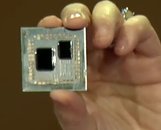
At its CES 2019 keynote, AMD unveiled two killer client-segment products, the Radeon VII graphics card, which beats the GeForce RTX 2080; and a sneak preview of the 3rd generation Ryzen socket AM4 processor based on the company's "Zen 2" microarchitecture. As part of the unveil, CEO Lisa Su demonstrated an 8-core/16-thread 3rd generation Ryzen prototype processor in a head-to-head CineBench nT face-off with the Intel Core i9-9900K processor, which has the same core-count. The Ryzen narrowly beat the Intel flagship. Following this, Dr. Su held up a de-lidded sibling of the processor that was tested, revealing not one, but two dies.
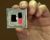
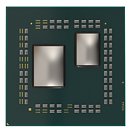
This confirms that AMD is taking the heterogeneous multi-chip module approach to building its 3rd generation Ryzen processors, much like its 2nd generation EPYC processors that were unveiled late last year. The MCM of the processor Dr. Su held up had two chips, the smaller chip is an 8-core CPU chiplet built on the 7 nm process, that appears to have the same die-size as the 8-core chiplets that make up the 64-core 2nd gen EPYC MCMs, the larger die is an I/O controller logic built on the 14 nm process. This die controls the memory, PCIe, and SoC connectivity of the package. We noticed something curious about the way the two dies are arranged on the package substrate.On close inspection of the substrate, we find that while the I/O controller die is somewhat centrally to the side of the package, the sole 8-core CPU chiplet is not located at a similar position (think Intel "Clarkdale" MCMs). On zooming in further, we find that just south of the 8-core CPU chiplet die, there appear to be blank bumps protruding over an area similar to that of a chiplet covered up by the outer layers of the substrate, leading us to conclude that the AM4 package is capable of three dies, an I/O controller, and two 8-core CPU chiplets. There very much will be a 16-core/32-thread Ryzen for the AM4 platform, and it's only a question of when.
The 16-core Ryzen AM4 MCM will be similar in concept to the larger 64-core SP3r2 EPYC/Threadripper MCMs: the CPU dies only pack the CPU cores and an InfinityFabric interface, while the I/O controller die is wired to multiple CPU dies, and manages the memory, PCIe, and SoC connectivity of the processor.
Interestingly, in the client-segment Intel dabbled with this concept a decade ago with "Clarkdale," which combined a 32 nm dual-core CPU die that spoke to a larger 65 nm die that controlled PCIe, memory, and an iGPU, with QPI serving as the interconnect between the two. Intel's requirements at the time were different. The company hadn't yet managed to put CPU and iGPU into a single die, and needed the iGPU to sit closer to the memory interface. The company would go onto fuse CPU and iGPU with the 32 nm "Sandy Bridge."
AMD's engineering bravado with "Matisse" also unlocks the possibility of the Ryzen "Raven Ridge" APU successor being an MCM with one 8-core chiplet, and an oversized I/O controller die that packs a "Vega" or "Navi" based iGPU, in addition to memory, PCIe, SoC, and the works. Dies on that package could be arranged differently from this.


40 Comments on AMD 3rd Gen Ryzen AM4 Package Capable of Two 8-core Chiplets
I think the bigger news is that AMD has fully caught up with Intel at IPC.
At 1:38-1:45 the light shines on it and is clearly visable.
Gordon goes on to say Lisa Su pretty much confirms they could have more then 8 cores.
100% designed for 16 cores on AM4!
Smoking !
Bring it faster AMD, my wallet is itching !
It's going to be a long 6 months waiting for this, which will be my first AMD system in 12 years.
Oh, and all nice to see AdoredTV being proved right again, despite all the negativity towards him.
Good guys AMD :toast:
I was actually thinking of Navi a bit in another thread AMD could have a I/O die with 6 chiplets similar to what a Vega 32 would be aka a completely cut in half Vega 64. They'd be better yields naturally and efficiency would be quite a bit better plus the waste heat easier to manage. Basically 6 smaller die Vega chips and one more monolithic I/O die chip sitting between all 6 of them 3 on each side of it. It would be a absolute powerhouse. I mean what does Vega 64 do for traditional ray tracing in terms of frame rates?
Cut that in half and presto no RTX gimmick just pure traditional ray tracing via brute force of essentially a chiplet render farm of sorts. Now with path tracing it could be interesting. We need to get to a point with ray tracing with path tracing though where you can apply that in real time to a scene based on like mipmap/LOD/Culling type behavior selectively for denoise. Simply making the more distant less important and visible scenes have a bit less denoise applied since it's less vital anyway.Not that surprised if they shrink that I/O die to 7nm they could squeeze in 3 chiplets alongside it.The gist of it is Intel got really complacent in recent years. I think we'll see something akin to C2D/C2Q transition from AMD64 in response eventually, but that kind of change doesn't happen overnight. Much like AMD64 kicked the pants out of Intel for awhile and like Ryzen is doing pretty well now. I'm just hoping neither company gets to complacent and that they both try to one up the other in tangible significant ways as opposed to oh hey here's a 2-3% performance boost for 100% of the cost of the last generation product lineup enjoy the price gouging.
-----
My concern is that when/if 12/16 core variants arrive, will the dual channel memory controller be enough? Many of the workloads which could utilize this many cores are very bandwidth intensive. I assume Ryzen 3 will use memory beyond DDR4-2933, but to my knowledge only DDR4-3200 is currently finalized by the JEDEC standard. And before anyone suggest overclocking memory, I would remind everyone that it's not a reliable solution.
Anyway, the benchmark conducted on CES was with DDR4-2666.
I mean people buying the 16-core models will likely not be buying them for gaming first, and I doubt they will lose any performance. Remember that the 2990WX loses in gaming only because it has "island dies" - it's not because of a lack of bandwidth, it's a lack of a decent connection to bandwidth. And even then, they have shown the 2990WX would perform only ~10% worse in games than the other Ryzen chips if Windows would schedule correctly.