Wednesday, January 23rd 2019

Bulldozer Core-Count Debate Comes Back to Haunt AMD
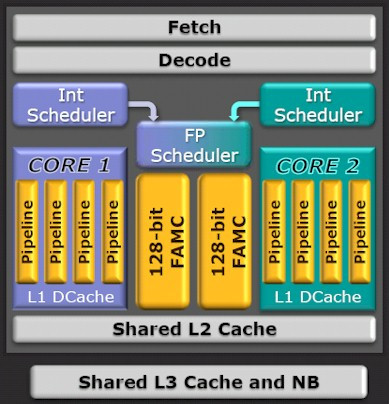
AMD in 2012 launched the FX-8150, the "world's first 8-core desktop processor," or so it says on the literal tin. AMD achieved its core-count of 8 with an unconventional CPU core design. Its 8 cores are arranged in four sets of two cores each, called "modules." Each core has its own independent integer unit and L1 data cache, while the two cores share a majority of their components - the core's front-end, a branch-predictor, a 64 KB L1 code cache, a 2 MB L2 cache, but most importantly, an FPU. There was much debate across tech forums on what constitutes a CPU core.
Multiprocessor-aware operating systems had to be tweaked on how to properly address a "Bulldozer" processor. Their schedulers would initially treat "Bulldozer" cores as fully independent (as conventional logic would dictate), until AMD noticed multi-threaded application performance bottlenecks. Eventually, Windows and various *nix kernels received updates to their schedulers to treat each module as a core, and each core as an SMT unit (a logical processor). The FX-8350 is a 4-core/8-thread processor in the eyes of Windows 10, for example. These updates improved the processors' performance but not before consumers started noticing that their operating systems weren't reporting the correct core-count. In 2015, a class-action lawsuit was filed against AMD for false marketing of FX-series processors. The wheels of that lawsuit are finally moving, after a 12-member Jury is set up to examine what constitutes a CPU core, and whether an AMD FX-8000 or FX-9000 series processor can qualify as an 8-core chip.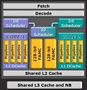
 US District Judge Haywood Gilliam of the District Court for the Northern District of California rejected AMD's claim that "a significant majority of" consumers understood what constitutes a CPU core, and that they had a fair idea of what they were buying when they bought AMD FX processors. AMD has two main options before it. The company can reach an agreement with the plaintiffs that could cost the company millions of Dollars in compensation; or fight it out in the Jury trial, by trying to prove to 12 members of the public (not necessarily from an IT background) what constitutes a CPU core and why "Bulldozer" qualifies as an 8-core silicon.
The plaintiffs and defendants each have a key technical argument. The plaintiffs could point out operating systems treating 8-core "Bulldozer" parts as 4-core/8-thread (i.e. each module as a core and each "core" as a logical processor); while the AMD could run multi-threaded floating-point benchmark tests to prove that a module cannot be simplified to the definition of a core. AMD's 2017 release of the "Zen" architecture sees a return to the conventional definition of a core, with each "Zen" core being as independent as an Intel "Skylake" core. We will keep an eye on this case.
Source:
The Register
Multiprocessor-aware operating systems had to be tweaked on how to properly address a "Bulldozer" processor. Their schedulers would initially treat "Bulldozer" cores as fully independent (as conventional logic would dictate), until AMD noticed multi-threaded application performance bottlenecks. Eventually, Windows and various *nix kernels received updates to their schedulers to treat each module as a core, and each core as an SMT unit (a logical processor). The FX-8350 is a 4-core/8-thread processor in the eyes of Windows 10, for example. These updates improved the processors' performance but not before consumers started noticing that their operating systems weren't reporting the correct core-count. In 2015, a class-action lawsuit was filed against AMD for false marketing of FX-series processors. The wheels of that lawsuit are finally moving, after a 12-member Jury is set up to examine what constitutes a CPU core, and whether an AMD FX-8000 or FX-9000 series processor can qualify as an 8-core chip.

The plaintiffs and defendants each have a key technical argument. The plaintiffs could point out operating systems treating 8-core "Bulldozer" parts as 4-core/8-thread (i.e. each module as a core and each "core" as a logical processor); while the AMD could run multi-threaded floating-point benchmark tests to prove that a module cannot be simplified to the definition of a core. AMD's 2017 release of the "Zen" architecture sees a return to the conventional definition of a core, with each "Zen" core being as independent as an Intel "Skylake" core. We will keep an eye on this case.
369 Comments on Bulldozer Core-Count Debate Comes Back to Haunt AMD
Also, 486DX is the first processor that supported both x86 and x87 instructions. It's processors before that which had x87 coprocessors.Core 2 Duo only shared L2 cache between cores:
Core 2 Quad had two of those packages on the same PCB. All four are independent, complete processors. The only cache that is necessary to the operation of a processor is L1.
Also, by AMD's definition, Core 2 Duo module would be a quad core because there's 4 ALUs. :pLook at any other processor on the market and there's a equal number of fetchers to cores. Bulldozer is an exception, not the rule.
Oh look, and Athlon 64 X2 slide from AMD!
See what they did there? Called the whole independent processor package an "execution core." AMD didn't draw a little box in the box saying this little integer bit here is the "core." :roll:
There's an enormous amount of hypocrisy by AMD on display here. In fact, there's really no references to the arithmetic units of a processor being called a "core" outside of Bulldozer's design.
Even Intel calls the whole independent processor a core. Here's a slide from Haswell:
As you can see, the industry has a very clear understanding of what a core is. AMD twisted that understanding to give the appearance of an edge against competing products. That's "false advertising." How is it okay for AMD to redefining the word in a way that is misleading to consumers?
For the record, one can make a CPU that has no addressable ALUs, only FPUs. There's really nothing an FPU can't do that an ALU can do. It is just slower and requires more transistors.Funny story there: disabling the FPU in the i486SX was similar as disabling a core in, for example, Zen. The FPU by far used the most die space on the 486 so instead of pitching chips that had a defect in the FPU, they disconnected it and sold it as an i486SX. The x87 instruction set and IEEE 754 standard was still in its infancy at the time so not much software used it.
The newest architecture that comes to my mind is IA-64. It was created from scratch long after IEEE 754. Is ALU and FPUs intrinsic to its cores? Why yes, of course:
Mmm, MIPS is kind of an oddball mostly designed for network routing. Does it have an FPU? R16000 does:
Doesn't matter what architecture you look at, cores are clearly defined and they are not just the arithmetic calculators like AMD claims*.
* Only when on the subject of Bulldozer, Steamroller, and Excavator.
I'm not saying a processor needs an FPU because that's completely dependent on the scenario in which it will be used. I'm saying that AMD had one definition of the word "core," changed it for Bulldozer through Excavator, and then went back to their original definition for Zen. That bit in the middle deserves a slap on the wrist.
And we started really with a pentium d. 64 x2, core 2, i5 and so on,
AMD significantly changed the formula but did not represent the differences in the advertising.
people like us who have an interest in this sort of stuff Made our own minds up about the processors. I decided they were not 8 cores. Some others agreed with amd.
But the issue is there genuinely is a difference. Even in all the "evidence" provided by the "they are 8 cores"people in this thread, amd admit they are not 8 traditional cores.
For the most part amd do not even refer to them as cores.
By AMD's own definition of a core from only the pentium D era they are not cores.
But amd advertised it as 8 cores to the masses who would have thought (it must be the same as a core 2, or a phenom, or other relevant multi core processor of the time, When it simply wasnt and still isnt.
Theres a reason why Phenoms and core 2 quads out performed or performed as well as a buldozer at the time, And theres a reason why i5's out perform them still to this day..
Im not going to say that its Only down to the layout of the die, because that simply isnt true. There were coner cutting and cost saving methods taken during manufacturing. Which did lead to potential performance losses which could ammount to low double digit performance drops compared to having designed some parts manually rather than via software.
But regardless of that the issue that the law suit is regarding remains.
people expected cores to mean the same thing as they did with phenoms and other similar cpus of the time. Sure most of them didn't know what that meant. and probably 80% of them dont even know how it is different.
But they are different and amd did not adequately advertise it as such..
You can say what you want..
But when people lose a law suit because they advertize 1billion bytes as a GB instead of 1.07billion, then "slight" differences do matter.
it also does not help that amd have changed back to traditional cores virtually admitting that the buldozer modules were infact worse than traditional cores.
You are making many assumptions about how things work internally that... just aren't so.
You are also cherry picking the fuck out of the facts hoping everyone else wont notice.
Claim you can't compare old FPU but keep pulling modern AVX2 FPU to first gen AVX fpu and repeatedly ignoring just 1 gen back.
Please just stop.
FPU is the same per int as in Thuban, but by organizing a pair of int into modules along with a dual fpu with shared fetcher it enables a flexibility that Thuban did not have and enables AVX across 2 FPU units. As per the scaling performance given (better than sandybridge) it is clear there are 8 fpu units.
Configuration is indeed different to enable AVX gen 1 support.
At the time, the shared resources was the only way to enable 8 cores on 32nm...
The FPU of zen is vastly superior because there is die room to enable it... just like moving to 7nm enables another doubling of cores...
You keep trying to look at 1 detail and declaring AMD was out to get people when it was a solid solution at the time.
1 module, 2 cores. 4mod/8 cores. It had a unique structure, there was no smt involved, and it outperformed the intel solution on multithreading... but due to the deeeep pipeline the ipc was decreased and required higher clocks to be competitive.
Ryzen 1800X|Zen|8c/16t|4.8
FX-9590|Vishera|4m/8t|1.2
Phenom II X6 1100T BE|Thuban|6c/6t|0.9
...an 8 core Thuban would have ended up having about the same number of transistors. There's a lot of thread management overhead in doing what AMD did with Excavator that simply did not exist in Thuban.Floating points were calculated using SMT.Only when you compare 1 AMD "module" with two threads compared to 1 Intel "core" with two threads. If you compare 1 Intel "core" to 1 AMD "integer core," Intel's solution is higher performing.AMD side graded to make their product more attractive to server and mainframe operators. It was designed to be cost effective in those use cases, not consumer use cases.
All the rest of your very fancy display amounts to flash/bang nitpicking. You did succeed in doing one thing though; you displayed for all to see that you understand that an execution unit does count as a full and complete core in and of it's own. It's good you're not an attorney as you would have effectively tanked your own case with that display and argument.
ArbitraryAffection gave excellent proof of this earlier:
There's only one fetch, one L1 instruction cache, and one decoder. Omit those components from either integer core and you have transistors that just look pretty in a picture. You cannot cleave a bulldozer module in two and have two functional processors. You can do so with virtually every other multi-core architecture out there.
What you see in that picture is a core by textbook definition. It just happens to be able to process two threads simultaneously when circumstances are favorable to doing so.
searchdatacenter.techtarget.com/definition/multi-core-processor
A core is synonymous with "CPU." Initial dual core processors were two CPUs sharing the same socket on the same bus, not unlike a dual socket, single CPU machine.
1800X can rightfully be called an 8 CPU machine on a single socket. FX-8350 can only be called a 4 CPU machine on a single socket. Because that gets awfully confusing, AMD, Intel, ARM, MIPS, etc. have taken to calling them "cores" instead so they can distinguish multi-socketed solutions from multi-CPUs on one socket solutions.
"Central Processing Unit main components"
No mentioning of independent fetch/decode stages, no load/store units, no FPUs, nothing that you argue constitutes a "independent processor" aka core. All I see is either generic "instruction decoder" or "timing and control".
You seem to be extremely fixated on the idea that CPU cores have to be independent processor. Let's see, independent meaning it can operate on it's own and fulfill all the functionalities that it could previously do while inside it's multi-core arrangement, right ?
The only thing that I can think of that fits that description is something like this : www.pcper.com/reviews/Processors/Intel-Atom-330-Dual-core-Processor-Review.
In this case you can totally pluck one core/processor out of the assembly and you can use it completely on it's own. It's undoubtedly self contained and self sufficient.
Not even AMD's upcoming chiplets designs would count as being made out of independent processors because they rely on external logic, which they share, to operate . Why wont you understand that independent processors do not exist anymore in the context of modern CPUs, they share caches, memory controllers , interconnects which, in particular are absolutely critical to their functionality. Intel even has a word for it : Uncore and it usually occupies a considerable portion of the die. It's also the reason why whenever Intel/AMD wants a new chip with less cores they to have redesign the whole damn thing instead of just "cleaving it in two".
accel.cs.vt.edu/files/lecture2.pdf
Breaks multicore processors into homogeneous (copy-pasta) and heterogenous (CELL is named but think SoC in general where there's many components put together to make a flexible whole).
Page 11: Dies, ObservationsPage 14: Multicore-present:The fetcher is what the operating system sees. This is why Windows 8/10 report FX-8350 as a "4 core," "8 logical processors" on 1 socket.
Have another (sourced from Intel no less):
www.ecs.umass.edu/ece/andras/courses/ECE668/Mylectures/Introduction_to_Multi_Core.pdf
Page 17, diagram and explanation of what it means to transition from one core to two. Area is 2x. Heterogenous cores by definition are copy-pasta and include all parts required to process instructions.
Page 18, Intel highlights the two heterogenous cores on Conroe.
Page 24, processor resources:
-Caches
-General Purpose Registers
-Segment Registers & TLB
-FP registers, XMM registers
-System Flags
-Control and Data registers, Debug registers, MSRs
-Many more
Page 25, explains differences between CMP, SMP, Hyper Threading, and Software Threading. Particularly relevant:
"Chip Multi Processing, refers to multiple physical core engines that have unique resources."
Bulldozer's FP registers and XMM registers are not unique resources to the integer cores, they're unique resources to the module. Bulldozer doesn't fit under SMP because that requires sharing all resources.
Page 26, "Core Architecture (Prescott)" diagram includes everything from instruction TLB to L2 cache. This mirrors AMD's slide showing an Excavator "core" next to a Zen "core."
Page 27, "Core Architecture (Xeon - Dual Core)" diagram which tells the same story as Prescott. The diagram only includes a single core but on the left most side of it, they have a label depicting "Second core" which means mirror what you see here on the other side of the L2 cache. More confirmation that a "core" is wholistic (fetch-decode-execute), not just what AMD calls an "integer core."
Page 28, "Multi-core platform (Freescale: embedded)" diagram which depicts two clear "e500-mc cores" with "accelerators" and "connectivity" attached to it via "CoreNet fabric."
Page 29, "Multi-core platform (RMI-XLR: embedded)" diagram depicting 8 clear cores on a "Memory Distributed Interconnect."
Page 30, "Tilera - 64 core CPU" diagram depicting 64 interconnected processors.
Page 34, "Tiled Design & Mesh Network" depicts Intel's 80-core Polaris showing each "core" as a "compute element" + "router"
Page 39, "Multi-core: Design Challenges" says "replicating cores improves productivity."First, I'll fix the diagram so it's relevant to Bulldozer:
Then I'll point that #1 proves my point:I assume IR stands for "Instruction Register." On all Bulldozer processors, this is part of the Fetch block which is shared for both threads. As far as #1 is concerned, you're only looking at one CPU.
#2 continues to drive that point home when considering Bulldozer (not Steamroller/Excavator):The Decode block is shared in Bulldozer so as far as this is concerned, there's only one CPU.
#3 is another task of Fetch block so rewind to what I said above. Two or three steps here dictate we're only dealing with one CPU. See how my tweaked diagram makes a whole lot of sense now?
Finally, step #4 and #5, we get to the sole components where the cycle deviates but only if the instruction doesn't include a floating point instruction otherwise it is back to shared which means #4 and #5 are part of the singular CPU.
TL;DR: At least 3 steps say Bulldozer is a single CPU and without those steps, those integer clusters know not what to do. Pretty clear case a module is a core.Bulldozer shares "instruction decoder" (literally, I didn't modify the diagram at all) and "timing and control" via "Core Interface Unit" (Core IF in diagram):
This diagram has been posted at least twice now. I believe it was sourced from Tom's Hardware which is cited in the lawsuit.
And before you retort that Bulldozer can do two threads simultaneously, remember that it hits blocking scenarios more often than dual-core (or more) processors do as mouacyk pointed out:Bulldozer underperforms independent cores/processors in c-ray, compress-7zip, npb BT.A, npb FT.B, nbp LU.A, nbp UA.A, and clomp when comparing Opteron 2384 to FX-8150. For example, in 7-zip, FX-8150 only did 48% better where Opteron 2384 did 102% better. 7zip, as far as I can tell, is very ALU and cache intensive.
1. Fetch
2. Decode
Both of which are shared in Bulldozer.
These are part of the control unit on Figure 5.1.I am not sure why but you seem to have a skewed understanding of independent here. There is absolutely no need for a core to be a a separate chip. Independent core/CPU means it is able to perform its function - execute instructions - independently. No more, no less. Instructions are fetched from somewhere else and results are stored somewhere else - generally either the data bus or cache depending on how the wider system is built.
...roughly, anyway. Take those numbers times the number of cores and you'll get an approximation of multithreading scaling.
I'll have to accept that you will never be able to use correct information to prove your points and you'll always skew facts.
Those citations do not help your position. They actually work against it.Exactly correct.And that is clearly being demonstrated.
Ford, you have lost this debate on merit and by providing citations against your position. Let it go. AMD is going to win this case.
More info: www.anandtech.com/show/2170/3
I get the strong impression that Tera-Scale is entirely incapable of ALU work: everything exposed is floating point. That said, it was a prototype meant to reach 1 TFLOP of dynamic compute power and that's exactly what it did.
Amazingly even the slides that you provided contradict some of your claims about shared resources :
"Functional units" aka execution units, which may contain there own separate logic as is the case with the FP scheduler in the Bulldozer module. And that was one of your main points on why Bullzoder wasn't an 8 core CPU. Try as you may, it seems you can never get away from these facts.
Edit: Looking at the whole page, pretty sure he was referring to Hyper-threading so two threads sharing the same ALUs and FPUs. Hyper-threading impacts caches, tlb, and btb. The line directly below it also strongly suggests Hyper-threading (tradeoff being transistors spent on improving utilization in one core versus adding another core). Fits like a glove but again, just an educated guess.Bulldozer is anything but "basic." :roll:
- You are right, Tera-Scale can be looked at both ways - calling these 80 units cores can be argued as well as whether Tera-Scale is even a general purpose CPU. Intel Tera-Scale is a specialized application processor, both the intended application as well as architecture is much closer to GPU than a CPU. It is also a much simpler VLIW architecture with very simple instruction set and execution units (couple FPUs). This has more than a few similarities to AMD's similarly named VLIW GPU architecture TeraScale - HD2000-HD4000 series :)
- A simple CPU may only need instruction and data passed into it and control logic can be minimal or nonexistent, especially the decode part.
- Bulldozer on the other hand is an x86 CPU. This is effectively a RISC processor masquerading as CISC. Fetch and Decode have a large part to play in its operation.
Intel mostly designed Tera-Scale to test the idea of high-speed interconnects. It will never find its way into a commercial product most likely because they can't convince anyone to create and maintain the operating system for it.
For the record: Tera-Scale "tiles" are definitely cores just as Bulldozer "modules" are definitely cores. Fetch -> decode -> execute. Both do that, and so does every other core. If you try to call Tera-Scale's FPMACs "cores" like you call Bulldozer's integer cluster "cores," you end up with the same incomplete understanding of what a core must do. FPMACs and integer clusters are glorified calculators--not processors. They can tell you 1+1=2 but they can't tell you 2 is an index into an array of values and whether the referenced value is odd or even and if odd, is it prime? That takes a processor, not a calculator.