Monday, April 27th 2020

AMD to Support DDR5, LPDDR5, and PCI-Express gen 5.0 by 2022, Intel First to Market with DDR5
AMD is expected to support the next-generation DDR5 memory standard by 2022, according to a MyDrivers report citing industry sources. We are close to a change in memory standards, with the 5-year old DDR4 memory standard beginning a gradual phase out over the next 3 years. Leading DRAM manufacturers such as SK Hynix have already hinted mass-production of the next-generation DDR5 memory to commence within 2020. Much like with DDR4, Intel could be the first to market with processors that support it, likely with its "Sapphire Rapids" Xeon processors. AMD, on the other hand, could debut support for the standard only with its "Zen 4" microarchitecture slated for 2021 technology announcements, with 2022 availability.
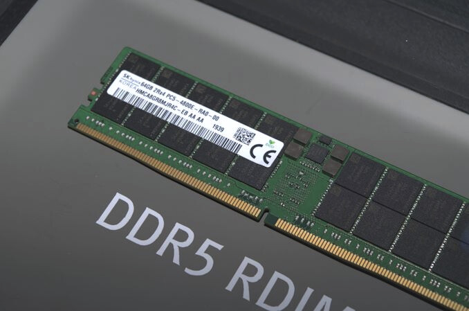
AMD "Zen 4" will see a transition to a new silicon fabrication process, likely TSMC 5 nm-class. It will be an inflection point for the company from an I/O standpoint, as it sees the introduction of DDR5 memory support across enterprise and desktop platforms, LPDDR5 on the mobile platform, and PCI-Express gen 5.0 across the board. Besides a generational bandwidth doubling, PCIe gen 5.0 is expected to introduce several industry-standard features that help with hyper-scalability in the enterprise segment, benefiting compute clusters with multiple scalar processors, such as AMD's CDNA2. Intel introduced many of these features with its proprietary CXL interconnect. AMD's upcoming "Zen 3" microarchitecture, scheduled for within 2020 with market presence in 2021, is expected to stick with DDR4, LPDDR4x, and PCI-Express gen 4.0 standards. DDR5 will enable data-rates ranging between 3200 to 8400 MHz, densities such as single-rank 32 GB UDIMMs, and a few new physical-layer features such as same-bank refresh.
Source:
MyDrivers
AMD "Zen 4" will see a transition to a new silicon fabrication process, likely TSMC 5 nm-class. It will be an inflection point for the company from an I/O standpoint, as it sees the introduction of DDR5 memory support across enterprise and desktop platforms, LPDDR5 on the mobile platform, and PCI-Express gen 5.0 across the board. Besides a generational bandwidth doubling, PCIe gen 5.0 is expected to introduce several industry-standard features that help with hyper-scalability in the enterprise segment, benefiting compute clusters with multiple scalar processors, such as AMD's CDNA2. Intel introduced many of these features with its proprietary CXL interconnect. AMD's upcoming "Zen 3" microarchitecture, scheduled for within 2020 with market presence in 2021, is expected to stick with DDR4, LPDDR4x, and PCI-Express gen 4.0 standards. DDR5 will enable data-rates ranging between 3200 to 8400 MHz, densities such as single-rank 32 GB UDIMMs, and a few new physical-layer features such as same-bank refresh.
45 Comments on AMD to Support DDR5, LPDDR5, and PCI-Express gen 5.0 by 2022, Intel First to Market with DDR5
SIPP memory was individual memory chips you had to add to the board. We had an old 8086 in school that had about a dozen or two of SIPPs mounted in it.
And again, contrarely to most DDR change, DDR5 is not just "Doubling the transfert speed while cutting in half the internal memory clock". This time, there are major design change in the memory itself that make any past comparaison useless.
All Ryzen did was lower the price of Intel's lineup. At least in the beginning, with the previously unknown (at the time) Zen architecture. Now, yes they did add more cores in direct competition with Ryzen, however it wasn't all because of Ryzen.
Am I the only one interested in seeing powerhouse APUs? I think it'd be amazing to have the option to abstain from the dGPU market altogether and the powerful SFF builds possible with such APUs would be legendary. I haven't even mentioned what they'd do for the mobile market.
Which, of course, is why I'm excited for DDR5 for APUs - 'cause it will actually happen, and will have huge benefits for iGPU performance. The same goes for LPDDR5 obviously.
wccftech.com/samsung-soc-amd-gpu-beat-snapdragon-865-adreno-650/
- I don't think interposers are suitable for smartphone/tablet applications, partly due to cost/complexity and partly due to durability: interposers are large and thin pieces of silicon, and at least in current implementations they would have significant risks of cracking if used in something that's likely to be dropped like a phone. Of course they could be strengthened, and any kind of SoC+HBM on interposer package for a phone/tablet is likely to be packaged in a ceramic (or at least epoxy) package that will help support the interposer, but it will still be significantly more brittle than any other mobile SoC. As for cost, not only is making the interposer relatively expensive, HBM also costs many time more than an off-the-shelf LPDDR package, and production costs with mounting both chips on the interposer and then packaging them would also be many times higher. I'm not sure if an interposer could be mounted directly to the phone motherboard or not, but at least all current implementations of interposers place them on a substrate first, adding thickness. Of course this will be somewhat offset by not having DRAM stacked on top of the SoC, but you would end up with a quite large, thick package for the SoC+DRAM - large enough that it might be difficult to fit on most phone motherboards. Implementing something like this in a laptop form factor would be far easier as the change in SoC form factor would be much smaller, and there's more space to work with in the first place. Durability concerns are also much lower in an implementation like that.
- Of course this could change with new packaging methods; if chip-on-chip stacking (rather than package-on-package or chip-on-interposer-on-substrate) finally arrives for high volume and high power implementations that could allow for HBM to be stacked directly on top of an SoC. HBM cost would still be an issue for mobile, but new packaging like this would make its use somewhat more likely.
- The "low-hanging fruit" comment regarding successors to Zen was referring to upcoming architectural improvements; we saw some of that addressed with Zen+ (cache improvements) and more of it with Zen 2. After all, as you work towards and eventually settle on a base design (that is finalized 1-1.5 years before it reaches retail) you will inevitably find areas (big or small) where it could be improved with various degrees of effort. Node improvements can of course help further improve things, but the two are not necessarily related.
- Silicon yields are absolutely affected by circuit design, but the specifics of this are extremely ... well, specific and fine-grained; any silicon design must be tweaked and tuned for the node it is designed to be manufactured on, but the specific design (as in: the actual layout that is to be etched into the silicon, not just the architectural layout) is also based off node-specific design libraries specifying how various types of transistors, interconnects, etc. are shaped and laid out. This is why transferring a chip design from one node to another is far from trivial - if the nodes are very different, it is essentially a brand new design even if the overall architecture is the same. In other words, you can't really compare the implementations of entirely different CPU designs on entirely different nodes beyond high-level overviews (unless you want to write a couple of Ph.D.s on the subject, I suppose). The reason why AMD managed to overtake Intel like they have with the current generation can be summed up as a confluence of various factors related in various ways: In terms of silicon manufacturing, AMD had access to a relatively mature 7nm node while Intel struggled to get their comparable 10nm node to work properly (not directly related to silicon designs). In terms of architecture, AMD improved the Zen design enough to surpass Skylake and its derivatives in IPC, while Intel was still using Skylake (holding off its new core designs for the perpetually delayed 10nm node which, as noted above, they were designed for, and redesigning them for 14nm would be a significant undertaking). And in terms of the combination of architecture and node, AMD could reap the rewards of an efficient architecture on an efficient node with better clock scaling than the previous node, while Intel had no recourse but to push clock speeds ever higher on their aging 14nm node, compounding AMD's efficiency lead while barely managing to keep up in absolute performance (and arguably not managing this in multithreaded workloads). This won't change until at least Tiger lake (mobile 10nm, reportedly actually working well) and Rocket Lake (14nm backport of 10nm Willow Cove core) arrive, but by that time AMD will have Zen 3 CPUs out at least in the desktop space.
- HBM doesn't relate much to this: Intel has already used HBM in a mobile chip after all (Kaby Lake-G) through its EMIB interconnect tech. If price is taken out of the picture, anyone can use HBM in any non-tiny form factor should they want to. AMD could make a HBM-equipped APU tomorrow (well, not technically tomorrow, it'd take time to implement in silicon) if they wanted to, they would just need to put a HBM PHY and controller in the APU and design and manufacture an interposer and package for it. For desktops this would be more challenging as it would be extremely difficult to fit this + a reasonably sized APU within the constraints of an AM4 package and its IHS - there isn't much area there. So it's also a question of balance: HBM would be meaningless if it could only be paired with an iGPU too small for it to be utilized properly. Still, cost and addressable markets (and therefore margins) is the biggest hindrance here. KBL-G saw just a handful of implementations, and an expensive APU isn't likely to be widely adopted if OEMs can get similar or better performance at a comparable price through separate CPUs and GPUs (which they are also far more familiar with designing cooling systems and motherboards for).
Is HBM essential to the changes made in the Zen architecture, or is it solely for the graphics (you mention cache, which is just memory, is that HBM caching? If so, then just because Intel hasn't successfully reaped rewards of it yet doesn't mean it isn't something won't have to do eventually (still thinking of the x64 issue), since Kaby Lake G was trying to use it for graphics anyway and not cpu..
It seems like if it is fundamental to the way forward space can be made for it even with a temporary generational protrusion like is done with the camera bumps; issues like cost and size have been just a matter of time and investment for scale and process improvement, and competition by Intel (or licensing from AMD like they did with x64 and like the Chinese have now done with x86 from AMD) would seem to only improve the problems of miniaturization and economization. Smartphone CPUs today outdo what the vacuum-tube computers that filled large rooms used to, after all.
If i understand you correctly, you're saying that the logic/architecture of the chip itself has to be remapped to any given node - is that because the foundry technique itself varies widely, or because of microscopic differences in from foundry to foundry built upon the same specifications? Is it just like, intel and amd don't know why one wafer-maker gets the yields it does but the foundry does have more ground knowledge and goes through a bunch of different iterations, and the logic guys just give them the file to print and work it out? Maybe just more circuit dense regions have different electrical properties than others under a given photo/heating/chemical process or something?
Yes, the top bin would have been a hexa-core today, if Ryzen hadn't appeared at all.