SK hynix Showcases Server and Storage Tech Strategies at HPE Discover 2025
SK hynix shared its technology roadmap, solution strategies, and AI cloud vision for leading the AI era at HPE Discover Las Vegas 2025 held from June 23-26. HPE Discover is a global technology conference hosted by Hewlett Packard Enterprise (HPE). This year's Las Vegas event highlighted the arrival of the AI era and its future possibilities. The conference featured a wide range of technical presentations, a networking program with demos and exhibitions, and hands-on training sessions such as the Tech Pro University and AI Developer Workshop.
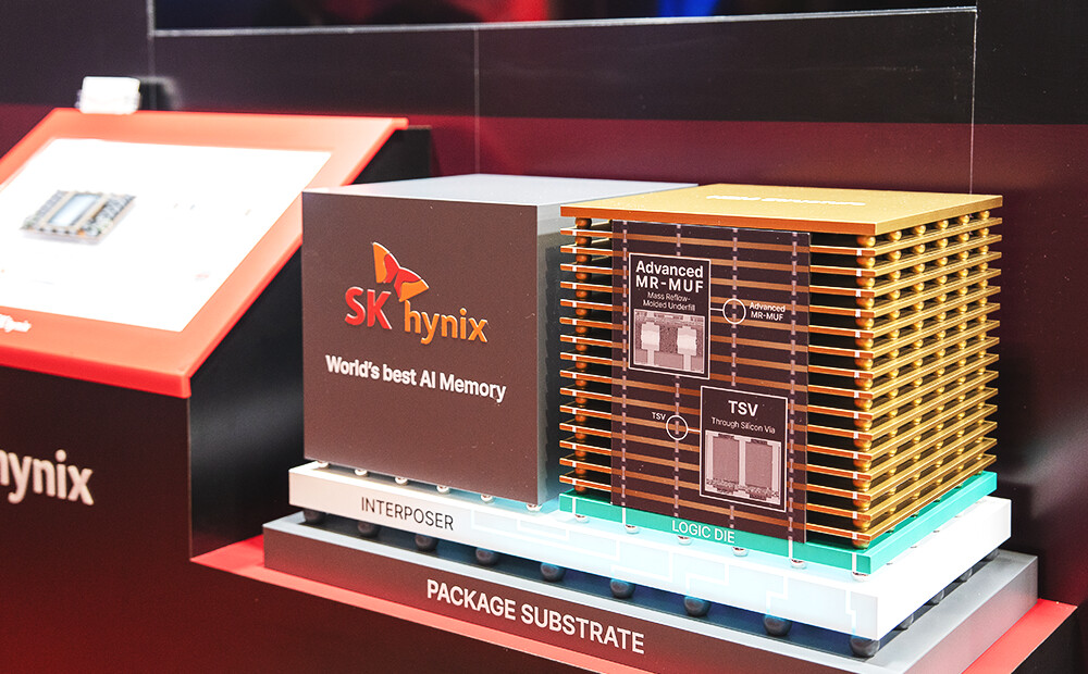
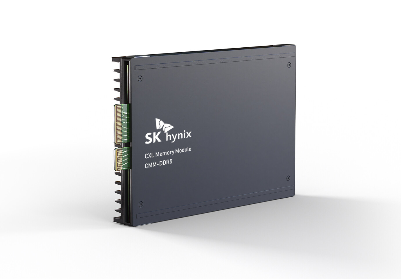
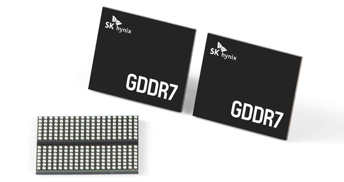
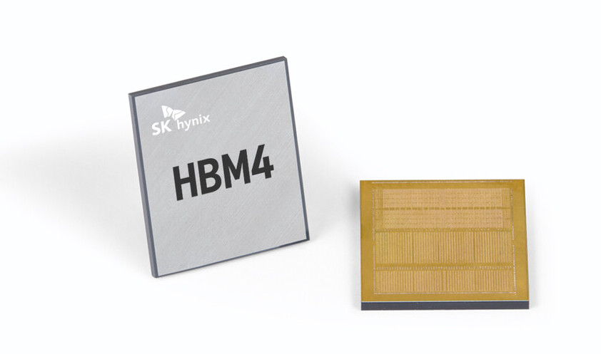
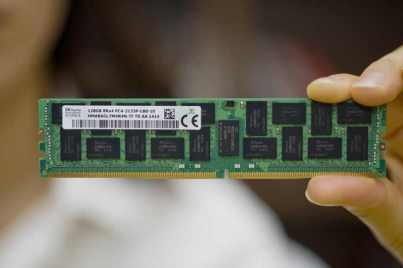
SK hynix showcased its technological leadership through presentations and exhibitions highlighting its next-generation AI memory, server, and storage solutions essential for developing AI infrastructure. The exhibition was divided into four key sections: HBM, Server DIMM, eSSDs and CMM (CXL Memory Module)-DDR5. Each section of the booth, which featured eye-catching designs including product mascots, presented key products and solutions.
SK hynix showcased its technological leadership through presentations and exhibitions highlighting its next-generation AI memory, server, and storage solutions essential for developing AI infrastructure. The exhibition was divided into four key sections: HBM, Server DIMM, eSSDs and CMM (CXL Memory Module)-DDR5. Each section of the booth, which featured eye-catching designs including product mascots, presented key products and solutions.