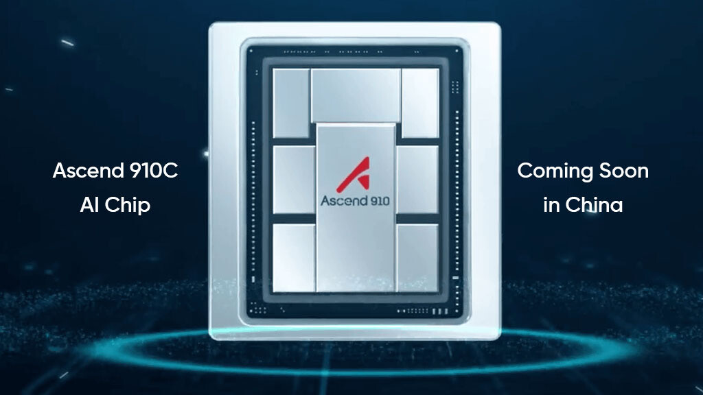
News Posts matching #5 nm

Return to Keyword Browsing

NVIDIA Confirms February 20 Availability Date of GeForce RTX 5070 Ti

NVIDIA's official GeForce Twitter handle just confirmed that the GeForce RTX 5070 Ti will be available from February 20, 2025. This is the third RTX 50-series "Blackwell" graphics card launch. The RTX 5070 Ti is positioned in the enthusiast segment considering its starting price of $749, with custom-design OC cards expected to be priced well above $800. Although officially being recommended for maxed out gameplay at WQHD (2560 x 1440) or ultrawide 3440 x 1440 resolutions, we expect the RTX 5070 Ti to be capable of gameplay at 4K UHD considering its predecessors, the RTX 4070 Ti and RTX 3070 Ti, each were at launch.

The GeForce RTX 5070 Ti is carved out from the same 5 nm "GB203" silicon that powers the RTX 5080 launched late last month. It is endowed with 70 out of 84 SM present on the silicon, which works out to 8,960 CUDA cores, 280 Tensor cores, 70 RT cores, 280 TMUs, and possibly 96 ROPs. The card gets 16 GB of [at least] 28 Gbps GDDR7 memory, giving it 896 GB/s of memory bandwidth on tap, a massive increase from the 12 GB and 504 GB/s of its predecessor. Then there are the Blackwell-exclusive technologies such as DLSS 4 Multi Frame Generation, Neural Rendering, Mega Geometry for ray tracing, and an updated display engine with support for DisplayPort 2.1b UHBR20. The picture NVIDIA used in its tweet shows an abstract-looking card, which could be a sign that there won't be a Founders Edition card of the RTX 5070 Ti.

Digital Foundry Believes that Nintendo Switch 2's Tegra T239 SoC is 8 nm Part

Yesterday, Nintendo officially unveiled its Switch 2 handheld via a first look video presentation. Featured content did not come as a surprise to many gaming enthusiasts—a steady flow of leaks have already revealed outer and inner workings. Earlier today, the Digital Foundry team has offered their collective opinion on Nintendo's formal announcement. Their roundtable discussion first focused on the Switch 2's physical appearance—mainly a showcased physical increase in size, when lined up against the preceding (standard) model. Conversation quickly moved onto technical matters—a topic that Nintendo normally avoids discussing. The video presentation included in-game footage of a next-gen Mario Kart title—Oliver Mackenzie (a contributing DF video producer/writer) was not impressed by this short demo's visual fidelity. He noted an absence of DLSS image enhancement—surprising, given that the rumored NVIDIA Tegra T239 SoC is capable of deploying this graphics technology.

John, Rich and Oliver then moved onto discussing recently leaked clock speeds and performance figures (in handheld and docked modes)—overall, they reckon that these numbers seem fitting for a hybrid system. They noticed that the handheld GPU clock was lower than expected—based on their judgement of the Switch 2's fairly capable integrated cooling solution. In the past, Digital Foundry theorized that the NVIDIA-designed Tegra T239 will be an 8 nanometer part—rumored to be built on Samsung 8 nm DUV foundry node. Newer gaming community-generated proposals have suggested a shift to Samsung's 5 nm EUV node—mostly based on the chipset's physical footprint. In sharp contrast, the Digital Foundry guys are sticking with their 8 nm theory. Richard Leadbetter (DF's founder) has previously attempted to simulate Switch 2-esque performance on readily available Ampere-based hardware—he could revisit and perform tests on a laptop that sports Team Green's GeForce RTX 2050 mobile GPU. He believes that the leaked CPU and GPU clocks (across both modes) present plausible evidence of 8 nm-level performance, cross-referenced with his team's past analysis of the system's PCB. Debates will inevitably rage on, but Rich insists that the end result will be an example of "Occam's razor." The Tegra T239's four (long alleged) Cortex A78 cores appeared to be running at a higher frequency in portable mode than in docked—suggesting some unknown factors; perhaps a switching on or off of cores (situation dependent). Leadbetter and Co. will be looking forward to getting a proper hands-on experience at Nintendo's April to June launch events.

Intel Arc B570 Graphics Card Available from Today

Intel today formally launched its second graphics card from the Arc "Battlemage" family, the Arc B570. This card is being launched at $220, or $30 cheaper than the Arc B580 from last month. With it, the company is looking to disrupt several products around the $200-mark, and probably even wage price wars below that mark. The card is designed to offer a 1080p AAA gaming experience enhanced with ray tracing, and the XeSS 2 feature set (super resolution, frame generation, and low-latency). Given that there is no RTX 3050 successor from NVIDIA, or anything from AMD around this price point, except older generation RX 6600-series products, the B570 could be poised to grab a chunk of the value-ended gaming PC market share.

The Arc B570 is based on the same 5 nm "BMG-G21" silicon that also powers the B580. It has 18 Xe cores enabled across five Render Slices, giving it 112 EU (execution units), or 2,240 unified shaders. Other key specs include 144 XMX cores for AI acceleration, 18 ray tracing units, 144 TMUs, and 60 ROPs. Perhaps the biggest differentiator between the B570 and B580 is memory, the B570 gets 10 GB of it, over a 160-bit wide GDDR6 memory bus, on which it runs 19 Gbps memory to yield 380 GB/s of memory bandwidth. With a total board power of 150 W compared to the 190 W of the B580, the B570 makes do with a single 8-pin PCIe power connector on even the factory overclocked parts. Intel has set a $220 baseline price, however, there is no reference design card, and the cheapest custom design cards start at $230, with an included factory overclock. We reviewed two such cards today, you can find them in the links below.

Read the TechPowerUp Reviews of the ASRock Arc B570 Challenger OC and the Sparkle Arc B570 Guardian OC.

TSMC Reports Record Q4 2024 Earnings with 37% YoY Growth

TSMC (TWSE: 2330, NYSE: TSM) today announced consolidated revenue of NT$868.46 billion, net income of NT$374.68 billion, and diluted earnings per share of NT$14.45 (US$2.24 per ADR unit) for the fourth quarter ended December 31, 2024. Year-over-year, fourth quarter revenue increased 38.8% while net income and diluted EPS both increased 57.0%. Compared to third quarter 2024, fourth quarter results represented a 14.3% increase in revenue and a 15.2% increase in net income. All figures were prepared in accordance with TIFRS on a consolidated basis.

In US dollars, fourth quarter revenue was $26.88 billion, which increased 37.0% year-over-year and increased 14.4% from the previous quarter. Gross margin for the quarter was 59.0%, operating margin was 49.0%, and net profit margin was 43.1%. In the fourth quarter, shipments of 3-nanometer accounted for 26% of total wafer revenue; 5-nanometer accounted for 34%; 7-nanometer accounted for 14%. Advanced technologies, defined as 7-nanometer and more advanced technologies, accounted for 74% of total wafer revenue.

Eighteen New Semiconductor Fabs to Start Construction in 2025

The semiconductor industry is expected to start 18 new fab construction projects in 2025, according to SEMI's latest quarterly World Fab Forecast report. The new projects include three 200 mm and fifteen 300 mm facilities, the majority of which are expected to begin operations from 2026 to 2027.

In 2025, the Americas and Japan are the leading regions with four projects each. The China and Europe & Middle East regions are each tied for third place with three planned construction projects. Taiwan has two planned projects, while Korea and Southeast Asia have one project each for 2025.

AMD Debuts Ryzen AI Max Series "Strix Halo" SoC: up to 16 "Zen 5" cores, Massive iGPU

AMD at the 2025 International CES debuted the Ryzen AI Max 300 series of mobile processors. These chips are designed to go up against the Apple M4 Pro, or the chip that powers the Apple MacBook Pro. The idea behind it is to provide leadership CPU and graphics performance from a single package, minimizing the PCB footprint from having a discrete GPU. In stark contrast, the Intel Core Ultra 200V "Lunar Lake," is designed more to go against the Apple M4, or the chips that power the latest MacBook Air but not quite the MacBook Pro. What sets "Strix Halo" functionally apart from "Lunar Lake" or even the M4 Pro, is that the AMD chip doesn't have memory-on-package (MoP), it relies on discrete LPDDR5X memory chips.

The "Strix Halo" processor is "Fire Range" on steroids. There are one or two "Zen 5" CCDs, for up to a 16-core/32-thread core configuration. Each of these "Zen 5" cores are unlike the ones on "Strix Point," in that they feature a fully unlocked AVX512 hardware pipeline (512-bit FP). The CCD shares a lavish 32 MB of L3 cache among 8 "Zen 5" cores. This is hardly the star attraction. Unlike "Fire Range," which features the small 6 nm client I/O die from "Granite Ridge," The new "Strix Halo" features a massive SoC die built on the 5 nm EUV foundry node. This packs the star attraction of the processor, it's oversized iGPU that has a massive 40 compute units (2,560 stream processors).

Nintendo Switch 2 PCB Leak Reveals an NVIDIA Tegra T239 Chip Optically Shrunk to 5nm

Nintendo Switch 2 promises to be this year's big (well small) gaming platform launch. It goes up against a growing ecosystem of handhelds based on x86-64 mobile processors running Windows, its main play would have to be offering a similar or better gameplay experience, but with better battery life, given that all of its hardware is purpose-built for a handheld console, and runs a highly optimized software stack; and the SoC forms a big part of this. Nintendo turned to NVIDIA for the job, given its graphics IP leadership, and its ability to integrate it with Arm CPU IP in a semi-custom chip. Someone with access to a Switch 2 prototype, likely an ISV, took the device apart, revealing the chip, a die-shrunk version of the Tegra T239 from 2023.

It's important to note that prototype consoles physically appear nothing like the final product, they're just designed so ISVs and game developers can validate them, and together with PC-based "official" emulation, set up the ability to develop or port games to the new platform. The Switch 2 looks very similar to the original Switch, it is a large tablet-like device, with detachable controllers. The largest chip on the mainboard is the NVIDIA Tegra T239. Nintendo Prime shared more details about the chip.

Rapidus Installs Japan's First ASML NXE:3800E EUV Lithography Machine

Rapidus Corporation, a manufacturer of advanced logic semiconductors, today announced the delivery and installation of ASML's EUV lithography equipment at its Innovative Integration for Manufacturing (IIM-1) foundry, an advanced semiconductor development and manufacturing fab currently under construction in Chitose, Hokkaido. To commemorate the installation, a ceremony was held at Portom Hall in the New Chitose Airport.

This is a significant milestone for Japan's semiconductor industry, marking the first time that an EUV lithography tool will be used for mass production in the country. In addition to the EUV lithography machinery, Rapidus will install additional complementary advanced semiconductor manufacturing equipment, as well as full automated material handling systems in its IIM-1 foundry to optimize 2 nm generation gate-all-around (GAA) semiconductor manufacturing.

TSMC and NVIDIA Reportedly in Talks to Bring "Blackwell" GPU Production to Arizona

TSMC is reportedly negotiating with NVIDIA to manufacture advanced "Blackwell" GPUs in its Arizona facility. First reported by Reuters, this partnership could mark another major shift in AI chip production toward US soil. The discussion centers around TSMC's Fab 21 in Phoenix, Arizona, specializing in 4 nm and 5 nm chip production. NVIDIA's Blackwell GPUs utilize TSMC's 4NP process technology, making the Arizona facility a technically viable production site. However, the proposed arrangement faces several logistical challenges. A key issue is the absence of advanced packaging facilities in the United States. There is Amkor that planned to do advanced packaging, but it's only scheduled to begin packaging in 2027. TSMC's sophisticated CoWoS packaging technology is currently available only in Taiwan. This means that chips manufactured in Arizona would need to be shipped back to Taiwan for final assembly, potentially increasing production costs.

While alternative solutions exist, such as redesigning the chips to use Intel's packaging technology or focusing on gaming GPU production in Arizona, these options present their own complications. Intel's packaging methods would likely increase costs, and the current absence of graphics card manufacturing infrastructure in the US makes domestic gaming GPU production less practical. Both TSMC and NVIDIA have declined to comment on the ongoing negotiations, as this is confidential information unknown to the public. Interestingly, TSMC's Arizona facility has already attracted a few more US firms for domestic manufacturing, like Apple, rumored to manufacture its A16 Bionic chip and AMD with high-performance designs, likely either EPYC or Instinct MI chips.

AMD Ryzen AI MAX 300 "Strix Halo" iGPU to Feature Radeon 8000S Branding

AMD Ryzen AI MAX 300-series processors, codenamed "Strix Halo," have been on in the news for close to a year now. These mobile processors combine "Zen 5" CPU cores with an oversized iGPU that offers performance rivaling discrete GPUs, with the idea behind these chips being to rival the Apple M3 Pro and M3 Max processors powering MacBook Pros. The "Strix Halo" mobile processor is an MCM that combines one or two "Zen 5" CCDs (some ones featured on "Granite Ridge" desktop processors and "Turin" server processors), with a large SoC die. This die is built either on the 5 nm (TSMC N5) or 4 nm (TSMC N4P) node. It packs a large iGPU based on the RDNA 3.5 graphics architecture, with 40 compute units (CU), and a 50 TOPS-class XDNA 2 NPU carried over from "Strix Point." The memory interface is a 256-bit wide LPDDR5X-8000 for sufficient memory bandwidth for the up to 16 "Zen 5" CPU cores, the 50 TOPS NPU, and the large 40 CU iGPU.

Golden Pig Upgrade leaked what looks like a company slide from a notebook OEM, which reveals the iGPU model names for the various Ryzen AI MAX 300-series SKUs. Leading the pack is the Ryzen AI MAX+ 395. This is a maxed out SKU with a 16-core/32-thread "Zen 5" CPU that uses two CCDs. All 16 cores are full-sized "Zen 5." The CPU has 64 MB of L3 cache (32 MB per CCD), each of the 16 cores has 1 MB of dedicated L2 cache. The iGPU is branded Radeon 8060S, it comes with all 40 CU (2,560 stream processors) enabled, besides 80 AI accelerators, and 40 Ray accelerators. The Ryzen AI MAX 390 is the next processor SKU, it comes with a 12-core/24-thread "Zen 5" CPU. Like the 395, the 390 is a dual-CCD processor, all 12 cores are full-sized "Zen 5." There's 64 MB of L3 cache, and 1 MB of L2 cache per core. The Radeon 8060S graphics solution is the same as the one on the Ryzen AI MAX+ 395, it comes with all 40 CU enabled.

M31 Launches USB4 IP for TSMC 5 nm Process

M31 Technology Corporation, a leading global provider of silicon intellectual property (IP), today announced that its cutting-edge USB4 IP has achieved silicon validation on TSMC's 5 nm (N5) process. The newly validated IP enhances data transfer capabilities for a new wave of mobile and portable devices. The announcement coincides with M31's participation in TSMC's 2024 Open Innovation Platform (OIP) Ecosystem Forum in Taiwan. This milestone underscores the close collaboration between M31 and TSMC, reflecting M31's commitment to advancing high-performance IP solutions by leveraging TSMC's innovative platform to drive next-generation connectivity.

M31's USB4 IP is built on the latest USB4 specification and represents a major leap in the evolution of USB architecture. It supports multi-protocol tunneling, enabling simultaneous transmission of multiple data types—such as USB, DisplayPort, and PCIe—over a single connection. The USB4 IP achieves 40 Gbps data transfer rates, significantly enhancing bandwidth associated with previous USB standards. The IP is fully compatible with USB 3.2, USB 2.0, and Thunderbolt 3, ensuring seamless integration with existing and future devices.

Samsung Electronics Announces Results for Third Quarter of 2024, 7 Percent Revenue Increase

Samsung Electronics today reported financial results for the third quarter ended Sept. 30, 2024. The Company posted KRW 79.1 trillion in consolidated revenue, an increase of 7% from the previous quarter, on the back of the launch effects of new smartphone models and increased sales of high-end memory products. Operating profit declined to KRW 9.18 trillion, largely due to one-off costs, including the provision of incentives in the Device Solutions (DS) Division. The strength of the Korean won against the U.S. dollar resulted in a negative impact on company-wide operating profit of about KRW 0.5 trillion compared to the previous quarter.

In the fourth quarter, while memory demand for mobile and PC may encounter softness, growth in AI will keep demand at robust levels. Against this backdrop, the Company will concentrate on driving sales of High Bandwidth Memory (HBM) and high-density products. The Foundry Business aims to increase order volumes by enhancing advanced process technologies. Samsung Display Corporation (SDC) expects the demand of flagship products from major customers to continue, while maintaining a quite conservative outlook on its performance. The Device eXperience (DX) Division will continue to focus on premium products, but sales are expected to decline slightly compared to the previous quarter.

Die-Shots of Intel Core Ultra "Arrow Lake-S" Surface, Thanks to ASUS

As Intel's Core Ultra "Arrow Lake-S" desktop processors near their launch, ASUS China put out a video presentation about its Z890 chipset motherboards ready for these processors, which included a technical run-down of Intel's first tile-based desktop processor, which included detailed die-shots of the various tiles. This is stuff that would require not just de-lidding the processor (removing the integrated heat-spreader), but also clearing up the top layers of the die to reveal the various components underneath.

The whole-chip die-shot gives us a bird's eye view of the four key logic tiles—Compute, Graphics, SoC, and I/O, sitting on top of the Foveros base tile. Our article from earlier this week goes into the die areas of the individual tiles, and the base tile. The Compute tile is built on the most advanced foundry node among the four tiles, the 3 nm TSMC N3B. Unlike the older generation "Raptor Lake-S" and "Alder Lake-S," the P-cores and E-core clusters aren't clumped into the two ends of the CPU complex. In "Arrow Lake-S," they follow a staggered layout, with a row of P-cores, followed by a row of E-core clusters, followed by two rows of P-cores, and then another row of E-core clusters, before the final row of P-cores, to achieve the total core-count of 8P+16E. This arrangement reduces concentration of heat when the P-cores are loaded (eg: when gaming), and ensures each E-core cluster is just one ringbus stop away from a P-core, which should improve thread-migration latencies. The central region of the tile has this ringbus, and 36 MB of L3 cache shared among the P-cores and E-core clusters.

Intel Arrow Lake-S Die Visibly Larger Than Raptor Lake-S, Die-size Estimated

As a quick follow-up to last week's "Arrow Lake-S" de-lidding by Madness727, we now have a line-up of a de-lidded Core Ultra 9 285K "Arrow Lake-S" processor placed next to a Core i9-14900K "Raptor Lake-S," and the Core i9-12900K "Alder Lake-S." The tile-based "Arrow Lake-S" is visibly larger than the two, despite being made on more advanced foundry nodes. Both the 8P+16E "Raptor Lake-S" and 8P+8E "Alder Lake-S" chips are built on the Intel 7 node (10 nm Enhanced SuperFin). The "Raptor Lake-S" monolithic chip comes with a die-area of 257 mm². The "Alder Lake-S" is physically smaller, at 215 mm². What sets the two apart isn't just the two additional E-core clusters on "Raptor Lake-S," but also larger caches—2 MB of L2 per P-core, increased form 1.25 MB/core, and 4 MB per E-core cluster, increased from 2 MB/cluster.

Thanks to high quality die-shots of the "Arrow Lake-S" by Madness727, we have our first die-area estimations by A Hollow Knight on Twitter. The LGA1851 fiberglass substrate has the same dimensions as the LGA1700 substrate. This is to ensure the socket retains cooler compatibility. Using geometrical measurements, the base tile of the "Arrow Lake-S" is estimated to be 300.9 mm² in area. The base-tile is a more suitable guideline for "die-area," since Intel uses filler tiles to ensure gaps in the arrangement of logic tiles are filled, and the chip aligns with the base-tile below. The base tile, built on an Intel 22 nm foundry node, serves like a silicon interposer, facilitating high-density microscopic wiring between the various logic tiles stacked on top, and an interface to the fiberglass substrate below.

TSMC Reports Third Quarter EPS Results, Expects Gross Profit Margin of Up to 59% in Q4 2024

TSMC today announced consolidated revenue of NT$759.69 billion (US$23.50 billion), net income of NT$325.26 billion (US$10.08 billion), and diluted earnings per share of NT$12.54 (US$1.94 per ADR unit) for the third quarter ended September 30, 2024. Year-over-year, third quarter revenue increased 39.0% while net income and diluted EPS both increased 54.2%. Compared to second quarter 2024, third quarter results represented a 12.8% increase in revenue and a 31.2% increase in net income. All figures were prepared in accordance with TIFRS on a consolidated basis.

In US dollars, third quarter revenue was $23.50 billion, which increased 36.0% year-over-year and increased 12.9% from the previous quarter. Gross margin for the quarter was 57.8%, operating margin was 47.5%, and net profit margin was 42.8%. In the third quarter, shipments of 3-nanometer accounted for 20% of total wafer revenue; 5-nanometer accounted for 32%; 7-nanometer accounted for 17%. Advanced technologies, defined as 7-nanometer and more advanced technologies, accounted for 69% of total wafer revenue.

Marvell Collaborates with Meta for Custom Ethernet Network Interface Controller Solution

Marvell Technology, Inc. (NASDAQ: MRVL), a leader in data infrastructure semiconductor solutions, today announced the development of FBNIC, a custom 5 nm network interface controller (NIC) ASIC in collaboration with Meta to meet the company's infrastructure and use case requirements. The FBNIC board design will also be contributed by Marvell to the Open Compute Project (OCP) community. FBNIC combines a customized network controller designed by Marvell and Meta, a co-designed board, and Meta's ASIC, firmware and software. This custom design delivers innovative capabilities, optimizes performance, increases efficiencies, and reduces the average time needed to resolve potential network and server issues.

"The future of large-scale, data center computing will increasingly revolve around optimizing semiconductors and other components for specific applications and cloud infrastructure architectures," said Raghib Hussain, President of Products and Technologies at Marvell. "It's been exciting to partner with Meta on developing their custom FBNIC on our industry-leading 5 nm accelerated infrastructure silicon platform. We look forward to the OCP community leveraging the board design for future innovations."

AMD to Become Major Customer of TSMC Arizona Facility with High-Performance Designs

After Apple, we just learned that AMD is the next company in line for US-based manufacturing in the TSMC Arizona facility. Industry analyst Tim Culpan reports that TSMC's Fab 21 in Arizona will soon be producing AMD's high-performance computing (HPC) processors, with tape out and manufacturing expected to commence on TSMC's 5 nm node next year. This move comes after previously reported Apple's A16 SoC production, which is already in progress at the facility and could see shipments before the end of this year, significantly ahead of the initially projected early 2025 schedule. The production of AMD's HPC chips in Arizona marks a crucial step towards establishing an AI-hardware supply chain operating entirely on American soil, which is expected to further expand with Intel Foundry and Samsung Texas facility.

Making HPC processors domestically serves as a significant milestone in reducing dependence on overseas semiconductor manufacturing and strengthening the US's position in the global chip industry. Adding to the momentum, TSMC and Amkor recently announced a collaboration on advanced packaging technologies, including Integrated Fan-Out (InFO) and Chip-on-Wafer-on-Substrate (CoWoS), which are vital for high-performance AI chips. However, as Amkor facilities are yet to be built, these chips are going to be shipped back to Taiwan for packaging before being integrated into the final product. Once the Amkor facility is up and running, Arizona will become the birthplace of fully manufactured and packaged silicon chips.

Samsung Starts Mass Production of PM9E1, Industry's Most Powerful PC SSD for AI

Samsung Electronics, the world leader in advanced memory technology, today announced it has begun mass-producing PM9E1, a PCIe 5.0 SSD with the industry's highest performance and largest capacity. Built on its in-house 5-nanometer (nm)-based controller and eighth-generation V-NAND (V8) technology, the PM9E1 will provide powerful performance and enhanced power efficiency, making it an optimal solution for on-device AI PCs. Key attributes in SSDs, including performance, storage capacity, power efficiency and security, have all been improved compared to its predecessor (PM9A1a).

"Our PM9E1 integrated with a 5 nm controller delivers industry-leading power efficiency and utmost performance validated by our key partners," said YongCheol Bae, Executive Vice President of Memory Product Planning at Samsung Electronics. "In the rapidly growing on-device AI era, Samsung's PM9E1 will offer a robust foundation for global customers to effectively plan their AI portfolios."

Canon Delivers FPA -1200NZ2C Nanoimprint Lithography System for Semiconductor Manufacturing to the Texas Institute for Electronics

Canon Inc. announced today that it will ship its most advanced lithography platform, the FPA-1200NZ2C nanoimprint lithography (NIL) system for semiconductor manufacturing, to the Texas Institute for Electronics (TIE), a Texas-based semiconductor consortium. Canon became the first in the world to commercialize a semiconductor manufacturing system that uses NIL technology, which forms circuit patterns in a different method from conventional projection exposure technology, when it released the FPA-1200NZ2C on October 13, 2023.

In contrast to conventional photolithography equipment, which transfers a circuit pattern by projecting it onto the resist coated wafer, the new product does it by pressing a mask imprinted with the circuit pattern into the resist on the wafer like a stamp. Because its circuit pattern transfer process does not go through an optical mechanism, fine circuit patterns on the mask can be faithfully reproduced on the wafer. With reduced power consumption and cost, the new system enables patterning with a minimum linewidth of 14 nm, equivalent to the 5 nm node that is required to produce most advanced logic semiconductors currently available.

Huawei Starts Shipping "Ascend 910C" AI Accelerator Samples to Large NVIDIA Customers

Huawei has reportedly started shipping its Ascend 910C accelerator—the company's domestic alternative to NVIDIA's H100 accelerator for AI training and inference. As the report from China South Morning Post notes, Huawei is shipping samples of its accelerator to large NVIDIA customers. This includes companies like Alibaba, Baidu, and Tencent, which have ordered massive amounts of NVIDIA accelerators. However, Huawei is on track to deliver 70,000 chips, potentially worth $2 billion. With NVIDIA working on a B20 accelerator SKU that complies with US government export regulations, the Huawei Ascend 910C accelerator could potentially outperform NVIDIA's B20 processor, per some analyst expectations.

If the Ascend 910C receives positive results from Chinese tech giants, it could be the start of Huawei's expansion into data center accelerators, once hindered by the company's ability to manufacture advanced chips. Now, with foundries like SMIC printing 7 nm designs and possibly 5 nm coming soon, Huawei will leverage this technology to satisfy the domestic demand for more AI processing power. Competing on a global scale, though, remains a challenge. Companies like NVIDIA, AMD, and Intel have access to advanced nodes, which gives their AI accelerators more efficiency and performance.

Samsung Starts Mass Production of PCle 5.0 PM9E1 SSD

Samsung Electronics Co., Ltd., the world leader in advanced memory technology, today announced it has begun mass producing PM9E1, a PCle 5.0 SSD with the industry's highest performance and largest capacity. Built on its in-house 5-nanometer (nm)-based controller and eighth-generation V-NAND (V8) technology, the PM9E1 will provide powerful performance and enhanced power efficiency, making it an optimal solution for on-device AI PCs. Key attributes in SSDs, including performance, storage capacity, power efficiency and security, have all been improved compared to its predecessor (PM9A1a).

"Our PM9E1 integrated with a 5 nm controller delivers industry-leading power efficiency and utmost performance validated by our key partners," said YongCheol Bae, Executive Vice President of Memory Product Planning at Samsung Electronics. "In the rapidly growing on-device AI era, Samsung's PM9E1 will offer a robust foundation for global customers to effectively plan their AI portfolios."

Microsoft Unveils New Details on Maia 100, Its First Custom AI Chip

Microsoft provided a detailed view of Maia 100 at Hot Chips 2024, their initial specialized AI chip. This new system is designed to work seamlessly from start to finish, with the goal of improving performance and reducing expenses. It includes specially made server boards, unique racks, and a software system focused on increasing the effectiveness and strength of sophisticated AI services, such as Azure OpenAI. Microsoft introduced Maia at Ignite 2023, sharing that they had created their own AI accelerator chip. More information was provided earlier this year at the Build developer event. The Maia 100 is one of the biggest processors made using TSMC's 5 nm technology, designed for handling extensive AI tasks on Azure platform.

Maia 100 SoC architecture features:
  • A high-speed tensor unit (16xRx16) offers rapid processing for training and inferencing while supporting a wide range of data types, including low precision data types such as the MX data format, first introduced by Microsoft through the MX Consortium in 2023.
  • The vector processor is a loosely coupled superscalar engine built with custom instruction set architecture (ISA) to support a wide range of data types, including FP32 and BF16.
  • A Direct Memory Access (DMA) engine supports different tensor sharding schemes.
  • Hardware semaphores enable asynchronous programming on the Maia system.

Imec Demonstrates Logic and DRAM Structures Using High NA EUV Lithography

Imec, a world-leading research and innovation hub in nanoelectronics and digital technologies, presents patterned structures obtained after exposure with the 0.55NA EUV scanner in the joint ASML-imec High NA EUV Lithography Lab in Veldhoven, the Netherlands. Random logic structures down to 9,5 nm (19 nm pitch), random vias with 30 nm center-to-center distance, 2D features at 22 nm pitch, and a DRAM specific lay out at P32nm were printed after single exposure, using materials and baseline processes that were optimized for High NA EUV by imec and its partners in the framework of imec's Advanced Patterning Program. With these results, imec confirms the readiness of the ecosystem to enable single exposure high-resolution High NA EUV Lithography.

Following the recent opening of the joint ASML-imec High NA EUV Lithography Lab in Veldhoven, the Netherlands, customers now have access to the (TWINSCAN EXE:5000) High NA EUV scanner to develop private High NA EUV use cases leveraging the customer's own design rules and lay outs.

Ampere Announces 512-Core AmpereOne Aurora CPU for AI Computing

Ampere has announced a significant update to its product roadmap, highlighting the upcoming 512-core AmpereOne Aurora processor. This new chip is specifically designed to address the growing demands of cloud-native AI computing.

The newly announced AmpereOne Aurora 512 cores processor integrates AI acceleration and on-chip High Bandwidth Memory (HBM), promising three times the performance per rack compared to current AmpereOne processors. Aurora is designed to handle both AI training and inference workloads, indicating Ampere's commitment to becoming a major player in the AI computing space.

Qualitas Semiconductor Develops First In-House PCIe 6.0 PHY IP

Qualitas Semiconductor Co., Ltd. has developed a new PCIe 6.0 PHY IP, marking a significant advance in computer interconnect technology. This new product, created using advanced 5 nm process technology is designed to meet the high-speed data transfer needs of the AI era. The Qualitas' PCIe PHY IP using 5 nm FinFet CMOS technology consists of hardmacro PMA and PCS compliant to PCIe Base 6.0 specification.

The PCIe 6.0 PHY IP can achieve transmission speeds up to 64GT/s per lane. When using all 16 lanes, it can transfer data at rates up to 256 GB/s. These speeds make it well-suited for data centers and self-driving car technologies, where rapid data processing is essential. Qualitas achieved this performance by implementing 100G PAM4 signaling technology. Highlighting the importance of the new IP, Qualitas CEO Dr. Duho Kim signaled the company's intent to continue pushing boundaries in semiconductor technology.
Return to Keyword Browsing
Feb 21st, 2025 20:52 EST change timezone

New Forum Posts

Popular Reviews

Controversial News Posts