News Posts matching #5 nm

Return to Keyword Browsing

SiFive's New High-Performance Processors Offer a Significant Upgrade for Wearable and Consumer Products

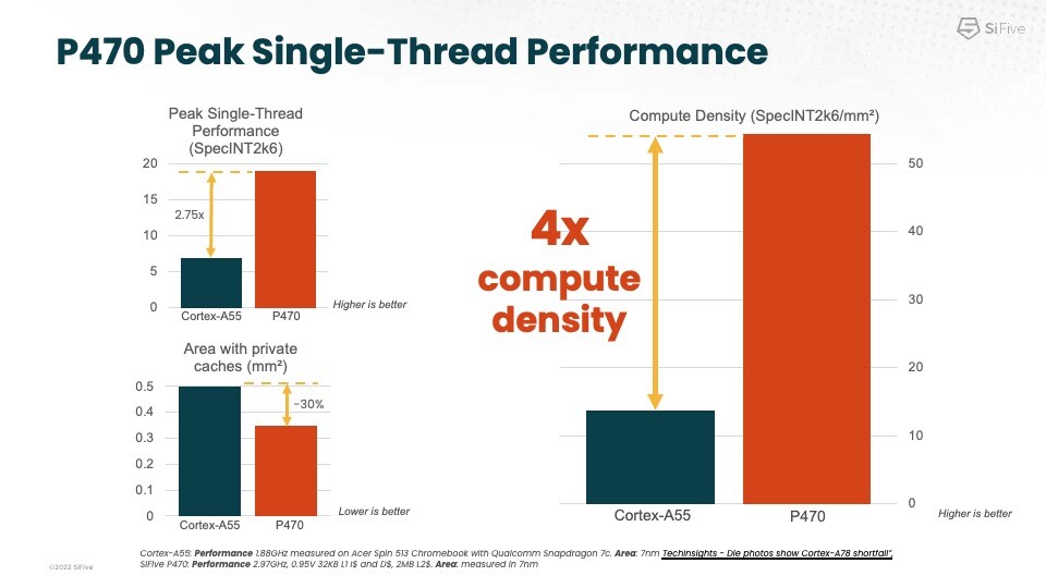
SiFive, Inc. the founder and leader of RISC-V computing, today announced two new products that address the need for high performance and efficiency in a small size in high volume applications like wearables, smart home, industrial automation, AR/VR, and other consumer devices. The SiFive Performance P670 and P470 RISC-V processors bring unparalleled compute performance and efficiency that is significantly raising the bar for innovative designs in these high-volume markets. The modern and innovative SiFive design methodologies bring raw compute density that is a substantial advantage for SiFive Performance products and also translates into significant cost savings for customers.

"The P670 and P470 are specifically designed for, and capable of handling the most demanding workloads for wearables and other advanced consumer applications. These new products offer powerful performance and compute density for companies looking to upgrade from legacy ISAs," said Chris Jones, SiFive VP of Product. "We have optimized these new RISC-V Vector enabled products to deliver the performance and efficiency improvements the industry has long been asking for, and we are in evaluations with a number of top-tier customers. Additionally, as the upstream enablement of RISC-V has started within the Android Open Source Project, (AOSP), designers will have unrivaled choice and flexibility as they consider the positive implications with that platform for future designs."

AMD Radeon RX 7000 RDNA3 To Launch Early December

AMD's next-generation Radeon RX 7000-series graphics cards based on the RDNA3 graphics architecture, are expected to launch in early-December 2022, according to greymon55, a reliable source with AMD leaks. The cards will be unveiled at a media event to be held on November 3, 2022, with market availability following a month after (between 1st to 5th December). The company is expected to take a top-down product-stack release cycle similar to that of NVIDIA, with the release of two of its top SKUs, the Radeon RX 7900 XTX and the RX 7900 XT. Both these cards are based on the 5 nm Navi 31 MCM GPU. This will be AMD's first client-graphics MCM GPU with more than one logic die. The company has a decade of experience with MCMs, but past generations have been one logic die surrounded with on-package HBM. Navi 31 has on-package logic chiplets, but discrete GDDR6 memory, like most other GPUs in the market today. It's rumored that the company is targeting a 100% performance uplift over the previous-generation, which means team-red is on the prowl to compete with NVIDIA's fastest SKUs, including the RTX 4090 and upcoming RTX 4080.

Intel's Next-Gen Desktop Platform Intros Socket LGA1851, "Meteor Lake-S" to Feature 6P+16E Core Counts

Keeping up with the cadence of two generations of desktop processors per socket, Intel will turn the page of the current LGA1700, with the introduction of the new Socket LGA1851. The processor package will likely have the same dimensions as LGA1700, and the two sockets may share cooler compatibility. The first processor microarchitecture to debut on LGA1851 will be the 14th Gen Core "Meteor Lake-S." These chips will feature a generationally lower CPU core-count compared to "Raptor Lake," but significantly bump the IPC on both the P-cores and E-cores.

"Raptor Lake" is Intel's final monolithic silicon client processor before the company pivots to chiplets built on various foundry nodes, as part of its IDM 2.0 strategy. The client-desktop version of "Meteor Lake," dubbed "Meteor Lake-S," will have a maximum CPU core configuration of 6P+16E (that's 6 performance cores with 16 efficiency cores). The chip has 6 "Redwood Cove" P-cores, and 16 "Crestmont" E-cores. Both of these are expected to receive IPC uplifts, such that the processor will end up faster (and hopefully more efficient) than the top "Raptor Lake-S" part. Particularly, it should be able to overcome the deficit of 2 P-cores.

IBM Artificial Intelligence Unit (AIU) Arrives with 23 Billion Transistors

IBM Research has published information about the company's latest development of processors for accelerating Artificial Intelligence (AI). The latest IBM processor, called the Artificial Intelligence Unit (AIU), embraces the problem of creating an enterprise solution for AI deployment that fits in a PCIe slot. The IBM AIU is a half-height PCIe card with a processor powered by 23 Billion transistors manufactured on a 5 nm node (assuming TSMC's). While IBM has not provided many details initially, we know that the AIU uses an AI processor found in the Telum chip, a core of the IBM Z16 mainframe. The AIU uses Telum's AI engine and scales it up to 32 cores and achieve high efficiency.

The company has highlighted two main paths for enterprise AI adoption. The first one is to embrace lower precision and use approximate computing to drop from 32-bit formats to some odd-bit structures that hold a quarter as much precision and still deliver similar result. The other one is, as IBM touts, that "AI chip should be laid out to streamline AI workflows. Because most AI calculations involve matrix and vector multiplication, our chip architecture features a simpler layout than a multi-purpose CPU. The IBM AIU has also been designed to send data directly from one compute engine to the next, creating enormous energy savings."

TSMC Cuts Back CAPEX Budget Despite Record Profits

Another quarter, another record breaking earnings report by TSMC, but it seems like the company has released that things are set to slow down sooner than initially expected and the company is hitting the brakes on some of its expansion projects. The company saw a 79.7 percent increase in profits compared to last year, with a profit of US$8.8 billion and a revenue of somewhere between US$19.9 to US$ 20.7 billion for the third quarter, which is a 47.9 percent bump compared to last year. TSMC's 5 nm nodes were the source for 28 percent of the revenues, followed by 26 percent for 7 nm nodes, 12 percent for 16 nm and 10 percent for 28 nm, with remaining nodes at 40 nm and larger making up for the remainder of the revenue. By platform, smartphone chips made up 41 percent, followed by High Performance Computing at 39 percent, IoT at 10 percent and automotive at five percent.

TSMC said it will cut back its CAPEX budget by around US$4 billion, to US$36 billion, compared to the earlier stated US$40 billion budget the company had set aside for expanding its fabs. Part of the reason for this is that TSMC is already seeing weaker demand for products manufactured using its N7 and N6 nodes, as the N7 node was meant to be a key part of the new fab in Kaohsiung in southern Taiwan. TSMC is expecting to start production on its first N3 node later this quarter and is expecting the capacity to be fully utilised for all of 2023. Supply is said to be exceeding demand, which TSMC said is partially to blame on tooling delivery issues. TSMC is expecting next year's revenue for its N3 node to be higher than its N5 node in 2020, although the revenue is said to be in the single digit percentage range. The N3E node is said to start production sometime in the second half of next year, or about a quarter earlier than expected. The N2 node isn't due to start production until 2025, but TSMC is already having very high customer engagement, so it doesn't look like TSMC is likely to suffer from a lack of business in the foreseeable future, as long as the company keeps delivering new nodes as planned.

AMD RDNA3 Radeon RX 7000 Flagship GPU PCB Sketched

Here's the very first sketch of an AMD RDNA3 Radeon RX 7000-series flagship graphics card with the "Navi 31" chip in the middle. This will be AMD's first chiplet-based GPU built on a philosophy similar to that of the Ryzen desktop and EPYC server processors. The main number crunching machinery that benefits the most from the latest foundry process, will be built on 5 nm logic chiplets (up to two of these on the "Navi 31," one of these on the "Navi 32"), while the components that don't really benefit from the latest process, such as the memory controllers, display/media accelerators, etc., will be disintegrated into chiplets built on a slightly older node, such as 6 nm. This way AMD gets to maximize its 5 nm allocation at TSMC, which it has to share among not just the logic tiles of RDNA3 GPUs, but also its "Zen 4" processors.

The top-dog "Navi 31" silicon is expected to feature a 384-bit wide GDDR6 memory interface, which is why you see 12 memory chips surrounding the GPU package. AMD is expected to deploy fast 19-21 Gbps class GDDR6 memory chips, as well as double-down on the Infinity Cache technology. The package looks like a GPU die surrounded by HBM stacks, but those are actually the memory/display chiplets. If this PCB is from an AMD reference design, it could be the biggest hint that AMD isn't switching over to the 12+4 pin ATX 12HPWR connector just yet, and could stick with three 8-pin PCIe connectors for power, just like the current RX 6950 XT. USB-C with DisplayPort passthrough could prominently feature with RDNA3 graphics cards, besides standard DisplayPort and HDMI connectors.

NVIDIA AD102 "Ada" Packs Over 75 Billion Transistors

NVIDIA's next-generation AD102 "Ada" GPU is shaping up to be a monstrosity, with a rumored transistor-count north of 75 billion. This would put over 2.6 times the 28.3 billion transistors of the current-gen GA102 silicon. NVIDIA is reportedly building the AD102 on the TSMC N5 (5 nm EUV) node, which offers a significant transistor-density uplift over the Samsung 8LPP (8 nm DUV) node on which the GA102 is built. The 8LPP offers 44.56 million transistors per mm² die-area (MTr/mm²), while the N5 offers a whopping 134 MTr/mm², which fits in with the transistor-count gain. This would put its die-area in the neighborhood of 560 mm². The AD102 is expected to power high-end RTX 40-series SKUs in the RTX 4090-series and RTX 4080-series.

AMD EPYC "Genoa" Zen 4 Product Stack Leaked

With its recent announcement of the Ryzen 7000 desktop processors, the action now shifts to the server, with AMD preparing a wide launch of its EPYC "Genoa" and "Bergamo" processors this year. Powered by the "Zen 4" microarchitecture, and contemporary I/O that includes PCI-Express Gen 5, CXL, and DDR5, these processors dial the CPU core-counts per socket up to 96 in case of "Genoa," and up to 128 in case of "Bergamo." The EPYC "Genoa" series represents the main trunk of the company's server processor lineup, with various internal configurations targeting specific use-cases.

The 96 cores are spread twelve 5 nm 8-core CCDs, each with a high-bandwidth Infinity Fabric path to the sIOD (server I/O die), which is very likely built on the 6 nm node. Lower core-count models can be built either by lowering the CCD count (ensuring more cores/CCD), or by reducing the number of cores/CCD and keeping the CCD-count constant, to yield more bandwidth/core. The leaked product-stack table below shows several of these sub-classes of "Genoa" and "Bergamo," classified by use-cases. The leaked slide also details the nomenclature AMD is using with its new processors. The leaked roadmap also mentions the upcoming "Genoa-X" processor for HPC and cloud-compute uses, which features the 3D Vertical Cache technology.

AMD "Zen 4" Dies, Transistor-Counts, Cache Sizes and Latencies Detailed

As we await technical documents from AMD detailing its new "Zen 4" microarchitecture, particularly the all-important CPU core Front-End and Branch Prediction units that have contributed two-thirds of the 13% IPC gain over the previous-generation "Zen 3" core, the tech enthusiast community is already decoding images from the Ryzen 7000 series launch presentation. "Skyjuice" presented the first annotation of the "Zen 4" core, revealing its large branch-prediction unit, enlarged micro-op cache, TLB, load/store unit, and dual-pumped 256-bit FPU that enables AVX-512 support. A quarter of the core's die-area is also taken up by the 1 MB dedicated L2 cache.

Chiakokhua (aka Retired Engineer) posted a table detailing the various caches and their latencies, comparing it with those of the "Zen 3" core. As AMD's Mark Papermaster revealed in the Ryzen 7000 launch event, the company has enlarged the micro-op cache of the core from 4 K entries to 6.75 K entries. The L1I and L1D caches remain 32 KB in size, each; while the L2 cache has doubled in size. The enlargement of the L2 cache has slightly increased latency, from 12 cycles to 14. Latency of the shared L3 cache is also up, from 46 cycles to 50 cycles. The reorder buffer (ROB) in the dispatch stage has been enlarged from 256 entries to 320 entries. The L1 branch target buffer (BTB) has increased in size from 1 KB to 1.5 KB.

AMD Confirms Optical-Shrink of Zen 4 to the 4nm Node in its Latest Roadmap

AMD in its Ryzen 7000 series launch event shared its near-future CPU architecture roadmap, in which it confirmed that the "Zen 4" microarchitecture, currently on the 5 nm foundry node, will see an optical-shrink to the 4 nm process in the near future. This doesn't necessarily indicate a new-generation CCD (CPU complex die) on 4 nm, it could even be a monolithic mobile SoC on 4 nm, or perhaps even "Zen 4c" (high core-count, low clock-speed, for cloud-compute); but it doesn't rule out the possibility of a 4 nm CCD that the company can use across both its enterprise and client processors.

The last time AMD hyphenated two foundry nodes for a single generation of the "Zen" architecture, was with the original (first-generation) "Zen," which debuted on the 14 nm node, but was optically shrunk and refined on the 12 nm node, with the company designating the evolution as "Zen+." The Ryzen 7000-series desktop processors, as well as the upcoming EPYC "Genoa" server processors, will ship with 5 nm CCDs, with AMD ticking it off in its roadmap. Chronologically placed next to it are "Zen 4" with 3D Vertical Cache (3DV Cache), and the "Zen 4c." The company is planning "Zen 4" with 3DV Cache both for its server- and desktop segments. Further down the roadmap, as we approach 2024, we see the company debut the future "Zen 5" architecture on the same 4 nm node, evolving into 3 nm on certain variants.

AMD Announces Ryzen 7000 Series "Zen 4" Desktop Processors

AMD today announced the Ryzen 7000 series "Zen 4" desktop processors. These debut the company's new "Zen 4" architecture to the market, increasing IPC, performance, with new-generation I/O such as DDR5 and PCI-Express Gen 5. AMD hasn't increased core-counts over the previous-generation, the Ryzen 5 series is still 6-core/12-thread, the Ryzen 7 8-core/16-thread, and Ryzen 9 either 12-core/24-thread, or 16-core/32-thread; but these are all P-cores. AMD is claiming a 13% IPC uplift generation over generation, which coupled with faster DDR5 memory, and CPU clock speeds of up to 5.70 GHz, give the Ryzen 7000-series processor an up to 29% single-core performance gain over the Ryzen 5000 "Zen 3."

At their press event, AMD showed us an up to 35% increase in gaming performance over the previous-generation, and an up to 45% increase in creator performance (which is where it gets the confidence to stick to its core-counts from). The "Zen 4" CPU core dies (CCDs) are built on the TSMC 5 nm EUV (N5) node. Even the I/O die sees a transition to 6 nm (N6), from 12 nm. The switch to 5 nm gives "Zen 4" 62 percent lower power for the same performance, or 49% more performance for the same power. versus the Ryzen 5000 series on 7 nm. The "Zen 4" core along with its dedicated L2 cache is 50% smaller, and 47% more energy efficient than the "Golden Cove" P-core of "Alder Lake."

AMD Ready with Zen 4 3DV Cache Chiplet, Expects to Repeat 5800X3D Magic Versus Raptor Lake

AMD is allegedly ready with a working "Zen 4" chiplet that has stacked 3D Vertical Cache (3DV cache) memory, which supplements the on-die L3 cache, and is found to massively improve gaming performance. "Moore's Law is Dead" reports that the Zen 4 + 3DV Cache chiplet will be used with various Ryzen 7000X3D SKUs, as well as special EPYC "Genoa" SKUs.

The 3DV Cache deployed with the "Zen 4" chiplet is a second-generation to the one on the "Zen 3 + 3DV cache" chiplet, and AMD has worked on a number of bandwidth and latency improvements, so it performs in-sync with the generationally-faster on-die L3 cache of the "Zen 4" chiplet. Unlike the CCD below it that's built on TSMC N5 (5 nm EUV), the L3D (the stacked die with the 3DV cache) is possibly be built on an older node, such as N6 (6 nm), since it only contains a slab of memory and doesn't warrant N5. "Moore's Law is Dead" reports that AMD expects to repeat the magic of the 5800X3D when it comes to gaming performance, and expects Ryzen 7000X3D processors to dominate Intel's 13th Gen "Raptor Lake" processors. This was echoed by another reliable source, greymon55.

AMD TSMC's Second Largest Customer for 5nm, More Resilient Than Intel to Face Downturns in the PC Industry: Report

AMD is now TSMC's second largest customer for its 5 nanometer N5 silicon fabrication node, according to a DigiTimes report. The Taiwan-based semiconductor industry observer also reports that AMD is more resilient than Intel in facing any downturns in the PC industry, in the coming few months. PC sales are expected to slump by as much as 15 percent in the near future, but the lower market-share compared to Intel; and the flexibility for AMD to move its CPU chips over to enterprise product to feed the growth in server processor segment, means that the company can ride over a bumpy road in the near future. The lower market-share translates to "lesser pain" from a slump compared to Intel. The report also says that embracing TSMC for processors "just in time" means that AMD has a front-row seat with product performance, time-to-market, yields, and delivery.

AMD is on the anvil of two major product launches on 5 nm, the Ryzen 7000 series "Raphael" desktop processors on August 30 (according to the report), and EPYC "Genoa" server processors in November 2022. The company is planning to refresh its notebook processor lineup in the first half of 2023, with "Dragon Range," and "Phoenix Point" targeting distinct market segments among notebooks. "Dragon Range" is essentially "Raphael" (5 nm chiplet + 6 nm cIOD) on a mobile-optimized BGA package, letting AMD cram up to 16 "Zen 4" cores, and take on Intel's high core-count mobile processors. The iGPU of "Dragon Range" will be basic, since designs based on this chip are expected to use discrete GPUs. "Phoenix Point" is a purpose-built mobile processor with up to 8 "Zen 4" cores, and a powerful iGPU based the RDNA3 architecture.

TSMC (Not Intel) Makes the Vast Majority of Logic Tiles on Intel "Meteor Lake" MCM

Intel's next-generation "Meteor Lake" processor is the first mass-production client processor to embody the company's IDM 2.0 manufacturing strategy—one of building processors with multiple logic tiles interconnected with Foveros and a base-tile (essentially an interposer). Each tile is built on a silicon fabrication process most suitable to it, so that the most advanced node could be reserved for the component that benefits from it the most. For example, while you need the SIMD components of the iGPU to be built on an advanced low-power node, you don't need its display controller and media engine to, and these could be relegated to a tile built on a less advanced node. This way Intel is able to maximize its use of wafers for the most advanced nodes in a graded fashion.

Japanese tech publication PC Watch has annotated the "Meteor Lake" SoC, and points out that the vast majority of the chip's tiles and logic die-area is manufactured on TSMC nodes. The MCM consists of four logic tiles—the CPU tile, the Graphics tile, the SoC tile, and the I/O tile. The four sit on a base tile that facilitates extreme-density microscopic wiring interconnecting the logic tiles. The base tile is built on the 22 nm HKMG silicon fabrication node. This tile lacks any logic, and only serves to interconnect the tiles. Intel has an active 22 nm node, and decided it has the right density for the job.

AMD Confirms Ryzen 7000 Launch Within Q3, Radeon RX 7000 Series Within 2022

AMD in its Q2-2022 financial results call with analysts, confirmed that the company's next-generation Ryzen 7000 desktop processors based on the "Zen 4" microarchitecture will debut this quarter (i.e. Q3-2022, or before October 2022). CEO Dr Lisa Su stated "Looking ahead, we're on track to launch our all-new 5 nm Ryzen 7000 desktop processors and AM5 platforms later this quarter with leadership performance in gaming and content creation."

The company also stated that its next-generation Radeon 7000 series GPUs based on the RDNA3 graphics architecture are on-track for launch "later this year," without specifying whether it meant this quarter, which could mean launch any time before January 2023. AMD is also on course to beating Intel to the next-generation of server processors with DDR5 and PCIe Gen 5 support, with its EPYC "Genoa" 96-core processor slated for later this year, as Intel struggles with a Q1-2023 general availability timeline for its Xeon Scalable "Sapphire Rapids" processor.

NVIDIA RTX 4090 "Ada" Scores Over 19000 in Time Spy Extreme, 66% Faster Than RTX 3090 Ti

NVIDIA's next-generation GeForce RTX 4090 "Ada" flagship graphics card allegedly scores over 19000 points in the 3DMark Time Spy Extreme synthetic benchmark, according to kopite7kimi, a reliable source with NVIDIA leaks. This would put its score around 66 percent above that of the current RTX 3090 Ti flagship. The RTX 4090 is expected to be based on the 5 nm AD102 silicon, with a rumored CUDA core count of 16,384. The higher IPC from the new architecture, coupled with higher clock speeds and power limits, could be contributing to this feat. Time Spy Extreme is a traditional DirectX 12 raster-only benchmark, with no ray traced elements. The Ada graphics architecture is expected to reduce the "cost" of ray tracing (versus raster-only rendering), although we're yet to see leaks of RTX performance, yet.

TSMC Reports Second Quarter EPS of NT$9.14

TSMC (TWSE: 2330, NYSE: TSM) today announced consolidated revenue of NT$534.14 billion, net income of NT$237.03 billion, and diluted earnings per share of NT$9.14 (US$1.55 per ADR unit) for the second quarter ended June 30, 2022. Year-over-year, second quarter revenue increased 43.5% while net income and diluted EPS both increased 76.4%. Compared to first quarter 2022, second quarter results represented an 8.8% increase in revenue and a 16.9% increase in net income. All figures were prepared in accordance with TIFRS on a consolidated basis.

In US dollars, second quarter revenue was $18.16 billion, which increased 36.6% year-over-year and increased 3.4% from the previous quarter. Gross margin for the quarter was 59.1%, operating margin was 49.1%, and net profit margin was 44.4%. In the second quarter, shipments of 5-nanometer accounted for 21% of total wafer revenue; 7- nanometer accounted for 30%. Advanced technologies, defined as 7-nanometer and more advanced technologies, accounted for 51% of total wafer revenue.

Semiconductor Fab Order Cancellations Expected to Result in Reduced Capacity Utilization Rate in 2H22

According to TrendForce investigations, foundries have seen a wave of order cancellations with the first of these revisions originating from large-size Driver IC and TDDI, which rely on mainstream 0.1X μm and 55 nm processes, respectively. Although products such as MCU and PMIC were previously in short supply, foundries' capacity utilization rate remained roughly at full capacity through their adjustment of product mix. However, a recent wave cancellations have emerged for PMIC, CIS, and certain MCU and SoC orders. Although still dominated by consumer applications, foundries are beginning to feel the strain of the copious order cancellations from customers and capacity utilization rate has officially declined.

Looking at trends in 2H22, TrendForce indicates, in addition to no relief from the sustained downgrade of driver IC demand, inventory adjustment has begun for smartphones, PCs, and TV-related peripheral components such as SoCs, CIS, and PMICs, and companies are beginning to curtail their wafer input plans with foundries. This phenomenon of order cancellations is occurring simultaneously in 8-inch and 12-inch fabs at nodes including 0.1X μm, 90/55 nm, and 40/28 nm. Not even the advanced 7/6 nm processes are immune.

NVIDIA to Cut Down TSMC 5nm Orders with the Crypto Gravy Train Derailed, AMD Could Benefit

NVIDIA is reportedly looking to reduce orders for 5 nm wafers from TSMC as it anticipates a significant drop in demand from both gamers and crypto-currency miners. Miners are flooding the market with used GeForce RTX 30-series graphics cards, which gamers are all too happy to buy, affecting NVIDIA's sales to both segments of the market. Before the crypto-currency crash of Q1-2022, NVIDIA had projected good sales of its next-generation GeForce GPUs, and prospectively placed orders for a large allocation of 5 nm wafers from TSMC. The company had switched back over to TSMC from Samsung, which makes 8 nm GPUs from the RTX 30-series.

With NVIDIA changing its mind on 5 nm orders, it is at the mercy of TSMC, which has made those allocations (and now faces a loss). It's incumbent on NVIDIA to find a replacement customer for the 5 nm volumes it wants to back out from. Chiakokhua (aka Retired Engineer), interpreted a DigiTimes article originally written in Chinese, which says that NVIDIA has made pre-payments to TSMC for its 5 nm allocation, and now wants to withdraw from some of it. TSMC is unwilling to budge—it could at best hold off shipments by a quarter to Q1-2023, allowing NVIDIA to get the market to digest inventory of 8 nm GPUs; and NVIDIA is responsible for finding replacement customers for the cancelled allocation.

Off-season Offsets Wafer Pricing Increase, 1Q22 Foundry Output Value Up 8.2% QoQ, Says TrendForce

According to TrendForce research, although demand for consumer electronics remains weak, structural growth demand in the semiconductor industry including for servers, high-performance computing, automotive, and industrial equipment has not flagged, becoming a key driver for medium and long term foundry growth. At the same time, due to robust wafer production at higher pricing in 1Q22, quarterly output value hit a new high for the 11th consecutive quarter, reaching US$31.96 billion, 8.2% QoQ, marginally less than the previous quarter. In terms of ranking, the biggest change is Nexchip surpassed Tower at the ninth position.

TSMC's across the board wafer hikes in 4Q21 on batches primarily produced in 1Q22 coupled with sustained strong demand for high-performance computing and better foreign currency exchange rates pushed TSMC's 1Q22 revenue to $17.53 billion, up 11.3% QoQ. Quarterly revenue growth by node was generally around 10% and the 7/6 nm and 16/12 nm processes posted the highest growth rate due to small expansions in production. The only instance of revenue decline came at the 5/4 nm process due to Apple's iPhone 13 entering the off season for production stocking.

AMD "Phoenix Point" Zen 4 Mobile Processor Powered Up

An engineering sample of AMD's next-generation Ryzen "Phoenix Point" mobile processor has been powered up, and made its first appearance on the Geekbench user-database. "Phoenix Point" is a monolithic silicon mobile processor built on the TSMC N5 (5 nm EUV) process, featuring "Zen 4" CPU cores, and a significantly faster iGPU based on the RDNA3 graphics architecture; along with a DDR5/LPDDR5 memory interface, and PCI-Express Gen 5.0 capability. An engineering sample with an 8-core/16-thread CPU, with the OPN code "100-000000709-23_N," hit the radar. AMD could debut Ryzen "Phoenix Point" in the first quarter of 2023, possibly with an International CES announcement.

AMD Plans Late-October or Early-November Debut of RDNA3 with Radeon RX 7000 Series

AMD is planning to debut its next-generation RDNA3 graphics architecture with the Radeon RX 7000 series desktop graphics cards, some time in late-October or early-November, 2022. This, according to Greymon55, a reliable source with AMD and NVIDIA leaks. We had known about a late-2022 debut for AMD's next-gen graphics, but now we have a finer timeline.

AMD claims that RDNA3 will repeat the feat of over 50 percent generational performance/Watt gains that RDNA2 had over RDNA. The next-generation GPUs will be built on the TSMC N5 (5 nm EUV) silicon fabrication process, and debut a multi-chip module design similar to AMD's processors. The logic dies with the GPU's SIMD components will be built on the most advanced node, while the I/O and display/media accelerators will be located in separate dies that can make do on a slightly older node.

AMD Said to Become TSMC's Third Largest Customer in 2023

Based on a report in the Taiwanese media, AMD is quickly becoming a key customer for TSMC and is expected to become its third largest customer in 2023. This is partially due to new orders that AMD has placed with TSMC for its 5 nm node. AMD is said to become TSMC's single largest customer for its 5 nm node in 2023, although it's not clear from the report how large of a share of the 5 nm node AMD will have.

The additional orders are said to be related to AMD's Zen 4 based processors, as well as its upcoming RDNA3 based GPUs. AMD is expected to be reaching a production volume of some 20,000 wafers in the fourth quarter of 2022, although there's no mention of what's expected in 2023. Considering most of AMD's products for the next year or two will all be based on TSMC's 5 nm node, this shouldn't come as a huge surprise though, as AMD has a wide range of new CPU and GPU products coming.

AMD's Second Socket AM5 Ryzen Processor will be "Granite Ridge," Company Announces "Phoenix Point"

AMD in its 2022 Financial Analyst Day presentation announced the codename for the second generation of Ryzen desktop processors for Socket AM5, which is "Granite Ridge." A successor to the Ryzen 7000 "Raphael," the next-generation "Granite Ridge" processor will incorporate the "Zen 5" CPU microarchitecture, with its CPU complex dies (CCDs) built on the 4 nm silicon fabrication node. "Zen 5" will feature several core-level designs as detailed in our older article, including a redesigned front-end with greater parallelism, which should indicate a much large execution stage. The architecture could also incorporate AI/ML performance enhancements as AMD taps into Xilinx IP to add more fixed-function hardware backing the AI/ML capabilities of its processors.

The "Zen 5" microarchitecture makes its client debut with Ryzen "Granite Ridge," and server debut with EPYC "Turin." It's being speculated that AMD could give "Turin" a round of CPU core-count increases, while retaining the same SP5 infrastructure; which means we could see either smaller CCDs, or higher core-count per CCD with "Zen 5." Much like "Raphael," the next-gen "Granite Ridge" will be a series of high core-count desktop processors that will feature a functional iGPU that's good enough for desktop/productivity, though not gaming. AMD confirmed that it doesn't see "Raphael" as an APU, and that its definition of an "APU" is a processor with a large iGPU that's capable of gaming. The company's next such APU will be "Phoenix Point."

AMD CDNA3 Architecture Sees the Inevitable Fusion of Compute Units and x86 CPU at Massive Scale

AMD in its 2022 Financial Analyst Day presentation unveiled its next-generation CDNA3 compute architecture, which will see something we've been expecting for a while—a compute accelerator that has a large number of compute units for scalar processing, and a large number of x86-64 CPU cores based on some future "Zen" microarchitecture, onto a single package. The presence of CPU cores on the package would eliminate the need for the system to have an EPYC or Xeon processor at its head, and clusters of Instinct CDNA3 processors could run themselves without the need for a CPU and its system memory.

The Instinct CDNA3 processor will feature an advanced packaging technology that brings various IP blocks together as chiplets, each based on a node most economical to it, without compromising on its function. The package features stacked HBM memory, and this memory is shared not just by the compute units and x86 cores, but also forms part of large shared memory pools accessible across packages. 4th Generation Infinity Fabric ties it all together.
Return to Keyword Browsing
Jul 12th, 2025 11:19 CDT change timezone

New Forum Posts

Popular Reviews

TPU on YouTube

Controversial News Posts