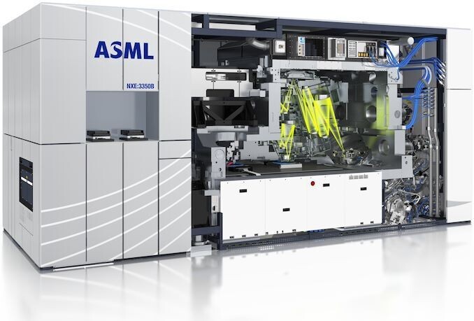
ASML Finishes Development of EUV Pellicles for Greater Sub-7nm Yields
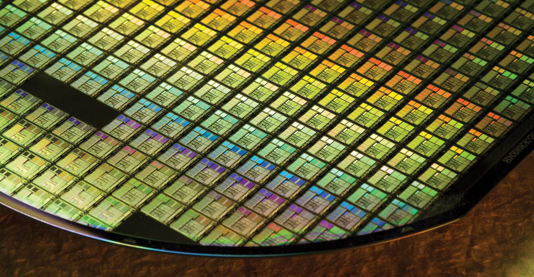
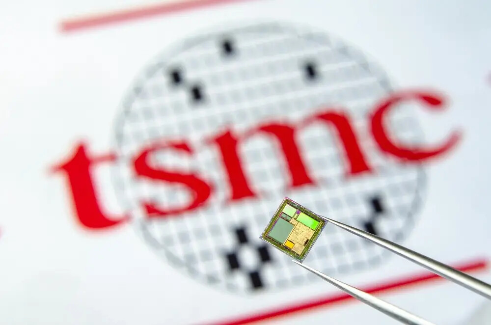
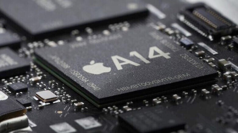
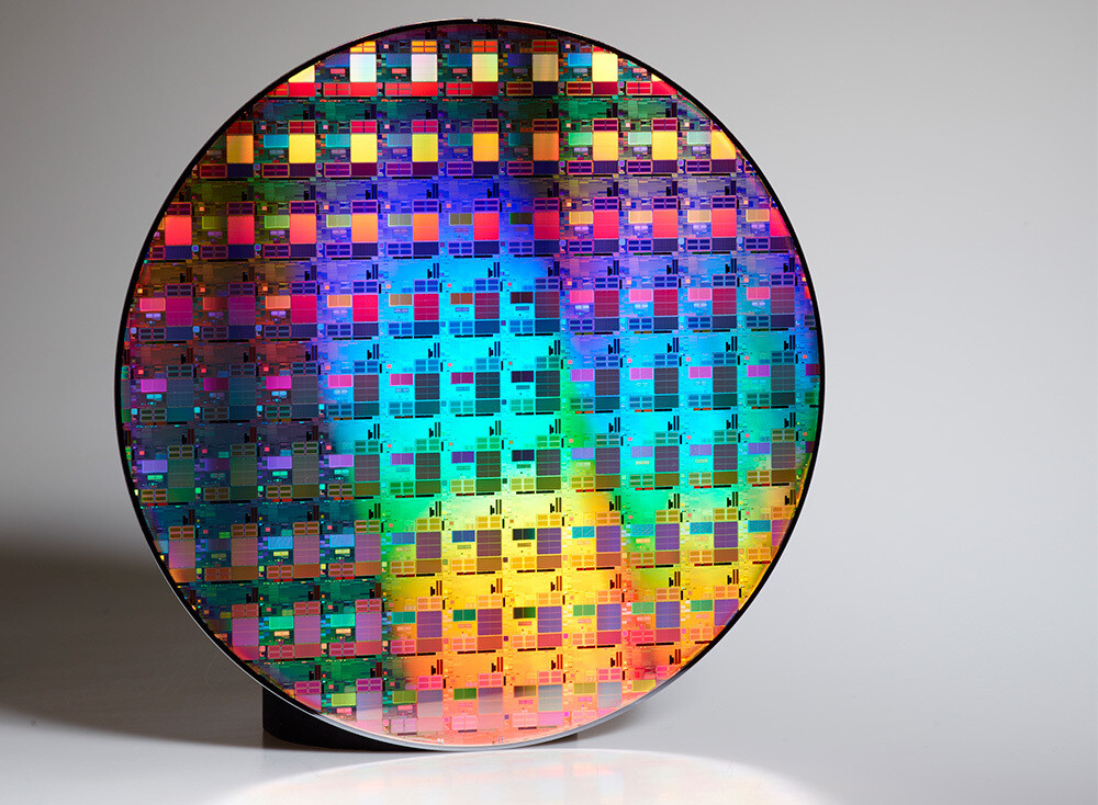
ASML has finally finished development of EUV (Extreme Ultra Violet) pellicles to be employed in manufacturing processes that use the most energetic frequency of visible light to etch semiconductors onto wafers. Pellicles have been used for decades in the industry, and they are basically ultra-thin membranes that protect photomasks during the etching process - impeding particles from depositing in the substrate, which could lead to defects at the wafer level for every subsequent patterning that is laid on top of the impurity. Manufacturers such as TSMC have deployed EUV-powered manufacturing processes, but they have had to toil with potentially lower yields and increased costs with wafer analysis so as to reduce chances of defects appearing.
It's been a long time coming for EUV-capable pellicles, because these have different requirements compared to their traditional, non-EUV counterparts. However, once they are available on the market, it's expected that all semiconductor manufacturers with bleeding-edge manufacturing processes integrate them into their production flows. These will allow for better yields, which in turn should reduce overall pricing for the manufacturing processes. As an example, these EUV masks could be deployed on TSMC's 7 nm, 6 nm, 5 nm, and so on and so on. Other players other than ASML are also finishing their pellicle design, so the industry will have multiple options to integrate into their processes.
It's been a long time coming for EUV-capable pellicles, because these have different requirements compared to their traditional, non-EUV counterparts. However, once they are available on the market, it's expected that all semiconductor manufacturers with bleeding-edge manufacturing processes integrate them into their production flows. These will allow for better yields, which in turn should reduce overall pricing for the manufacturing processes. As an example, these EUV masks could be deployed on TSMC's 7 nm, 6 nm, 5 nm, and so on and so on. Other players other than ASML are also finishing their pellicle design, so the industry will have multiple options to integrate into their processes.