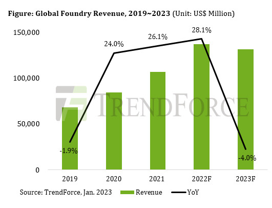
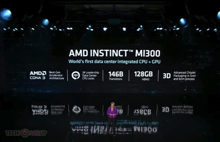
News Posts matching #5 nm

Return to Keyword Browsing

AMD Confirms Ryzen 7000 Launch Within Q3, Radeon RX 7000 Series Within 2022

AMD in its Q2-2022 financial results call with analysts, confirmed that the company's next-generation Ryzen 7000 desktop processors based on the "Zen 4" microarchitecture will debut this quarter (i.e. Q3-2022, or before October 2022). CEO Dr Lisa Su stated "Looking ahead, we're on track to launch our all-new 5 nm Ryzen 7000 desktop processors and AM5 platforms later this quarter with leadership performance in gaming and content creation."

The company also stated that its next-generation Radeon 7000 series GPUs based on the RDNA3 graphics architecture are on-track for launch "later this year," without specifying whether it meant this quarter, which could mean launch any time before January 2023. AMD is also on course to beating Intel to the next-generation of server processors with DDR5 and PCIe Gen 5 support, with its EPYC "Genoa" 96-core processor slated for later this year, as Intel struggles with a Q1-2023 general availability timeline for its Xeon Scalable "Sapphire Rapids" processor.

NVIDIA RTX 4090 "Ada" Scores Over 19000 in Time Spy Extreme, 66% Faster Than RTX 3090 Ti

NVIDIA's next-generation GeForce RTX 4090 "Ada" flagship graphics card allegedly scores over 19000 points in the 3DMark Time Spy Extreme synthetic benchmark, according to kopite7kimi, a reliable source with NVIDIA leaks. This would put its score around 66 percent above that of the current RTX 3090 Ti flagship. The RTX 4090 is expected to be based on the 5 nm AD102 silicon, with a rumored CUDA core count of 16,384. The higher IPC from the new architecture, coupled with higher clock speeds and power limits, could be contributing to this feat. Time Spy Extreme is a traditional DirectX 12 raster-only benchmark, with no ray traced elements. The Ada graphics architecture is expected to reduce the "cost" of ray tracing (versus raster-only rendering), although we're yet to see leaks of RTX performance, yet.

TSMC Reports Second Quarter EPS of NT$9.14

TSMC (TWSE: 2330, NYSE: TSM) today announced consolidated revenue of NT$534.14 billion, net income of NT$237.03 billion, and diluted earnings per share of NT$9.14 (US$1.55 per ADR unit) for the second quarter ended June 30, 2022. Year-over-year, second quarter revenue increased 43.5% while net income and diluted EPS both increased 76.4%. Compared to first quarter 2022, second quarter results represented an 8.8% increase in revenue and a 16.9% increase in net income. All figures were prepared in accordance with TIFRS on a consolidated basis.

In US dollars, second quarter revenue was $18.16 billion, which increased 36.6% year-over-year and increased 3.4% from the previous quarter. Gross margin for the quarter was 59.1%, operating margin was 49.1%, and net profit margin was 44.4%. In the second quarter, shipments of 5-nanometer accounted for 21% of total wafer revenue; 7- nanometer accounted for 30%. Advanced technologies, defined as 7-nanometer and more advanced technologies, accounted for 51% of total wafer revenue.

Semiconductor Fab Order Cancellations Expected to Result in Reduced Capacity Utilization Rate in 2H22

According to TrendForce investigations, foundries have seen a wave of order cancellations with the first of these revisions originating from large-size Driver IC and TDDI, which rely on mainstream 0.1X μm and 55 nm processes, respectively. Although products such as MCU and PMIC were previously in short supply, foundries' capacity utilization rate remained roughly at full capacity through their adjustment of product mix. However, a recent wave cancellations have emerged for PMIC, CIS, and certain MCU and SoC orders. Although still dominated by consumer applications, foundries are beginning to feel the strain of the copious order cancellations from customers and capacity utilization rate has officially declined.

Looking at trends in 2H22, TrendForce indicates, in addition to no relief from the sustained downgrade of driver IC demand, inventory adjustment has begun for smartphones, PCs, and TV-related peripheral components such as SoCs, CIS, and PMICs, and companies are beginning to curtail their wafer input plans with foundries. This phenomenon of order cancellations is occurring simultaneously in 8-inch and 12-inch fabs at nodes including 0.1X μm, 90/55 nm, and 40/28 nm. Not even the advanced 7/6 nm processes are immune.

NVIDIA to Cut Down TSMC 5nm Orders with the Crypto Gravy Train Derailed, AMD Could Benefit

NVIDIA is reportedly looking to reduce orders for 5 nm wafers from TSMC as it anticipates a significant drop in demand from both gamers and crypto-currency miners. Miners are flooding the market with used GeForce RTX 30-series graphics cards, which gamers are all too happy to buy, affecting NVIDIA's sales to both segments of the market. Before the crypto-currency crash of Q1-2022, NVIDIA had projected good sales of its next-generation GeForce GPUs, and prospectively placed orders for a large allocation of 5 nm wafers from TSMC. The company had switched back over to TSMC from Samsung, which makes 8 nm GPUs from the RTX 30-series.

With NVIDIA changing its mind on 5 nm orders, it is at the mercy of TSMC, which has made those allocations (and now faces a loss). It's incumbent on NVIDIA to find a replacement customer for the 5 nm volumes it wants to back out from. Chiakokhua (aka Retired Engineer), interpreted a DigiTimes article originally written in Chinese, which says that NVIDIA has made pre-payments to TSMC for its 5 nm allocation, and now wants to withdraw from some of it. TSMC is unwilling to budge—it could at best hold off shipments by a quarter to Q1-2023, allowing NVIDIA to get the market to digest inventory of 8 nm GPUs; and NVIDIA is responsible for finding replacement customers for the cancelled allocation.

Off-season Offsets Wafer Pricing Increase, 1Q22 Foundry Output Value Up 8.2% QoQ, Says TrendForce

According to TrendForce research, although demand for consumer electronics remains weak, structural growth demand in the semiconductor industry including for servers, high-performance computing, automotive, and industrial equipment has not flagged, becoming a key driver for medium and long term foundry growth. At the same time, due to robust wafer production at higher pricing in 1Q22, quarterly output value hit a new high for the 11th consecutive quarter, reaching US$31.96 billion, 8.2% QoQ, marginally less than the previous quarter. In terms of ranking, the biggest change is Nexchip surpassed Tower at the ninth position.

TSMC's across the board wafer hikes in 4Q21 on batches primarily produced in 1Q22 coupled with sustained strong demand for high-performance computing and better foreign currency exchange rates pushed TSMC's 1Q22 revenue to $17.53 billion, up 11.3% QoQ. Quarterly revenue growth by node was generally around 10% and the 7/6 nm and 16/12 nm processes posted the highest growth rate due to small expansions in production. The only instance of revenue decline came at the 5/4 nm process due to Apple's iPhone 13 entering the off season for production stocking.

AMD "Phoenix Point" Zen 4 Mobile Processor Powered Up

An engineering sample of AMD's next-generation Ryzen "Phoenix Point" mobile processor has been powered up, and made its first appearance on the Geekbench user-database. "Phoenix Point" is a monolithic silicon mobile processor built on the TSMC N5 (5 nm EUV) process, featuring "Zen 4" CPU cores, and a significantly faster iGPU based on the RDNA3 graphics architecture; along with a DDR5/LPDDR5 memory interface, and PCI-Express Gen 5.0 capability. An engineering sample with an 8-core/16-thread CPU, with the OPN code "100-000000709-23_N," hit the radar. AMD could debut Ryzen "Phoenix Point" in the first quarter of 2023, possibly with an International CES announcement.

AMD Plans Late-October or Early-November Debut of RDNA3 with Radeon RX 7000 Series

AMD is planning to debut its next-generation RDNA3 graphics architecture with the Radeon RX 7000 series desktop graphics cards, some time in late-October or early-November, 2022. This, according to Greymon55, a reliable source with AMD and NVIDIA leaks. We had known about a late-2022 debut for AMD's next-gen graphics, but now we have a finer timeline.

AMD claims that RDNA3 will repeat the feat of over 50 percent generational performance/Watt gains that RDNA2 had over RDNA. The next-generation GPUs will be built on the TSMC N5 (5 nm EUV) silicon fabrication process, and debut a multi-chip module design similar to AMD's processors. The logic dies with the GPU's SIMD components will be built on the most advanced node, while the I/O and display/media accelerators will be located in separate dies that can make do on a slightly older node.

AMD Said to Become TSMC's Third Largest Customer in 2023

Based on a report in the Taiwanese media, AMD is quickly becoming a key customer for TSMC and is expected to become its third largest customer in 2023. This is partially due to new orders that AMD has placed with TSMC for its 5 nm node. AMD is said to become TSMC's single largest customer for its 5 nm node in 2023, although it's not clear from the report how large of a share of the 5 nm node AMD will have.

The additional orders are said to be related to AMD's Zen 4 based processors, as well as its upcoming RDNA3 based GPUs. AMD is expected to be reaching a production volume of some 20,000 wafers in the fourth quarter of 2022, although there's no mention of what's expected in 2023. Considering most of AMD's products for the next year or two will all be based on TSMC's 5 nm node, this shouldn't come as a huge surprise though, as AMD has a wide range of new CPU and GPU products coming.

AMD's Second Socket AM5 Ryzen Processor will be "Granite Ridge," Company Announces "Phoenix Point"

AMD in its 2022 Financial Analyst Day presentation announced the codename for the second generation of Ryzen desktop processors for Socket AM5, which is "Granite Ridge." A successor to the Ryzen 7000 "Raphael," the next-generation "Granite Ridge" processor will incorporate the "Zen 5" CPU microarchitecture, with its CPU complex dies (CCDs) built on the 4 nm silicon fabrication node. "Zen 5" will feature several core-level designs as detailed in our older article, including a redesigned front-end with greater parallelism, which should indicate a much large execution stage. The architecture could also incorporate AI/ML performance enhancements as AMD taps into Xilinx IP to add more fixed-function hardware backing the AI/ML capabilities of its processors.

The "Zen 5" microarchitecture makes its client debut with Ryzen "Granite Ridge," and server debut with EPYC "Turin." It's being speculated that AMD could give "Turin" a round of CPU core-count increases, while retaining the same SP5 infrastructure; which means we could see either smaller CCDs, or higher core-count per CCD with "Zen 5." Much like "Raphael," the next-gen "Granite Ridge" will be a series of high core-count desktop processors that will feature a functional iGPU that's good enough for desktop/productivity, though not gaming. AMD confirmed that it doesn't see "Raphael" as an APU, and that its definition of an "APU" is a processor with a large iGPU that's capable of gaming. The company's next such APU will be "Phoenix Point."

AMD CDNA3 Architecture Sees the Inevitable Fusion of Compute Units and x86 CPU at Massive Scale

AMD in its 2022 Financial Analyst Day presentation unveiled its next-generation CDNA3 compute architecture, which will see something we've been expecting for a while—a compute accelerator that has a large number of compute units for scalar processing, and a large number of x86-64 CPU cores based on some future "Zen" microarchitecture, onto a single package. The presence of CPU cores on the package would eliminate the need for the system to have an EPYC or Xeon processor at its head, and clusters of Instinct CDNA3 processors could run themselves without the need for a CPU and its system memory.

The Instinct CDNA3 processor will feature an advanced packaging technology that brings various IP blocks together as chiplets, each based on a node most economical to it, without compromising on its function. The package features stacked HBM memory, and this memory is shared not just by the compute units and x86 cores, but also forms part of large shared memory pools accessible across packages. 4th Generation Infinity Fabric ties it all together.

AMD RDNA3 Offers Over 50% Perf/Watt Uplift Akin to RDNA2 vs. RDNA; RDNA4 Announced

AMD in its 2022 Financial Analyst Day presentation claimed that it will repeat the over-50% generational performance/Watt uplift feat with the upcoming RDNA3 graphics architecture. This would be a repeat of the unexpected return to the high-end and enthusiast market-segments of AMD Radeon, thanks to the 50% performance/Watt uplift of the RDNA2 graphics architecture over RDNA. The company also broadly detailed the various new specifications of RDNA3 that make this possible.

To begin with, RDNA3 debuts on the TSMC N5 (5 nm) silicon fabrication node, and will debut a chiplet-based approach that's somewhat analogous to what AMD did with its 2nd Gen EPYC "Rome" and 3rd Gen Ryzen "Matisse" processors. Chiplets packed with the GPU's main number-crunching and 3D rendering machinery will make up chiplets, while the I/O components, such as memory controllers, display controllers, media engines, etc., will sit on a separate die. Scaling up the logic dies will result in a higher segment ASIC.

AMD EPYC "Bergamo" 128-core Processor Based on Same SP5 Socket as "Genoa"

AMD is launching two distinct classes of next-generation enterprise processors, the 4th Generation EPYC "Genoa" with CPU core-counts up to 96-core/192-thread; and the new EPYC "Bergamo" with a massive 128-core/256-thread compute density. Pictures of the "Genoa" MCM are already out in the wild, revealing twelve "Zen 4" CCDs built on 5 nm, and a new-generation sIOD (I/O die) that's very likely built on 6 nm. The fiberglass substrate of "Genoa" already looks crowded with twelve chiplets, making us wonder if AMD needed a larger package for "Bergamo." Turns out, it doesn't.

In its latest Corporate presentation, AMD reiterated that "Bergamo" will be based on the same SP5 (LGA-6096) package as "Genoa." This would mean that the company either made room for more CCDs, or the CCDs themselves are larger in size. AMD states that "Bergamo" CCDs are based on the "Zen 4c" microarchitecture. Details about "Zen 4c" are scarce, but from what we gather, it is a cloud-optimized variant of "Zen 4" probably with the entire ISA of "Zen 4," and power characteristics suited for high-density cloud environments. These chiplets are built on the same TSMC N5 (5 nm EUV) process as the regular "Zen 4" CCDs.

AMD Unveils 5 nm Ryzen 7000 "Zen 4" Desktop Processors & AM5 DDR5 Platform

AMD today unveiled its next-generation Ryzen 7000 desktop processors, based on the Socket AM5 desktop platform. The new Ryzen 7000 series processors introduce the new "Zen 4" microarchitecture, with the company claiming a 15% single-threaded uplift over "Zen 3" (16-core/32-thread Zen 4 processor prototype compared to a Ryzen 9 5950X). Other key specs about the architecture put out by AMD include a doubling in per-core L2 cache to 1 MB, up from 512 KB on all older versions of "Zen." The Ryzen 7000 desktop CPUs will boost to frequencies above 5.5 GHz. Based on the way AMD has worded their claims, it seems that the "+15%" number includes IPC gains, plus gains from higher clocks, plus what the DDR4 to DDR5 transition achieves. With Zen 4, AMD is introducing a new instruction set for AI compute acceleration. The transition to the LGA1718 Socket AM5 allows AMD to use next-generation I/O, including DDR5 memory, and PCI-Express Gen 5, both for the graphics card, and the M.2 NVMe slot attached to the CPU socket.

Much like Ryzen 3000 "Matisse," and Ryzen 5000 "Vermeer," the Ryzen 7000 "Raphael" desktop processor is a multi-chip module with up to two "Zen 4" CCDs (CPU core dies), and one I/O controller die. The CCDs are built on the 5 nm silicon fabrication process, while the I/O die is built on the 6 nm process, a significant upgrade from previous-generation I/O dies that were built on 12 nm. The leap to 5 nm for the CCD enables AMD to cram up to 16 "Zen 4" cores per socket, all of which are "performance" cores. The "Zen 4" CPU core is larger, on account of more number-crunching machinery to achieve the IPC increase and new instruction-sets, as well as the larger per-core L2 cache. The cIOD packs a pleasant surprise—an iGPU based on the RDNA2 graphics architecture! Now most Ryzen 7000 processors will pack integrated graphics, just like Intel Core desktop processors.

AMD Ryzen 7000U "Phoenix" Processor iGPU Matches RTX 3060 Laptop GPU Performance: Rumor

AMD is planning a massive integrated graphics performance uplift for its next-generation Ryzen 7000U mobile processors. Codenamed "Phoenix," this SoC will feature a CPU based on the "Zen 4" microarchitecture with a higher CPU core count than the Intel alternative of the time; and an iGPU based on the RDNA3 graphics architecture. AMD is planning to endow this with the right combination of a CU count and engine clocks, to result in performance that roughly matches the NVIDIA GeForce RTX 3060 Laptop GPU, a popular performance-segment discrete GPU for notebooks, according to greymon55. Other highlights of "Phoenix" include a DDR5 + LPDDR5 memory interface, and PCI-Express Gen 5. The SoC is expected to be built on the TSMC N5 (5 nm) process, and debut in 2023.

NVIDIA AD102 and AMD Navi 31 in a Race to Reach 100 TFLOPs FP32 First

A technological race is brewing between NVIDIA and AMD over which brand's GPU reaches the 100 TFLOP/s peak FP32 throughput mark first. AMD's TeraScale graphics architecture and the "RV770" silicon, were the first to hit the 1 TFLOP/s mark, way back in 2008. It would take 14 years for this figure to reach 100 TFLOP/s for flagship GPUs. NVIDIA's next generation big GPU based on the "Ada Lovelace," the AD102, is the green team's contender for the 100 TFLOP/s mark, according to kopite7kimi. To achieve this, all 144 streaming multiprocessors (SM) or 18,432 CUDA cores, of the AD102 will have to be enabled.

From the red team, the biggest GPU based on the next-generation RDNA3 graphics architecture, "Navi 31," could offer peak FP32 throughput of 92 TFLOP/s according to greymon55, which gives AMD the freedom to create special SKUs running at high engine clocks, just to reach the 100 TFLOP/s mark. The Navi 31 silicon is expected to triple the compute unit count over its predecessor, resulting in 15,360 stream processors. Both the AD102 and Navi 31 are expected to be built on the same TSMC N5 (5 nm EUV) node, and product launches for both are expected by year-end.

Samsung Says Future Fab Nodes Are On Time, no Yield Issues on Current Nodes

Despite rumours of both production issues and node delays, Samsung has assured its shareholders during its first quarter conference call, that the company is on track. Its yield rate from its 5 nm node was said to have entered maturity, meaning that yields have entered Samsung's expected levels. However, Samsung did admit that its 4 nm node had seen some delays with the ramp up, but it has now entered the expected yield rate curve. The company is also working on an new R&D line for its upcoming 3 nm node, but didn't go into any further details.

As for Samsung's DRAM products, there were rumours that its 12 nm 1b process node had hit some snags and that the company was going to skip ahead to its 1c node, something the company denied. Samsung added that the development of 1b was proceeding stably and that the 1c node is expected to be done on schedule. The company also said that media reports of issues at Samsung's foundry business were overblown and that order books are full, which is why some of its customers have had to produce additional parts with TSMC. Samsung's foundry business reportedly saw an increase in operating profit of 50 percent compared to last year, as well as an increase in revenue of 19 percent.

AMD MI300 Compute Accelerator Allegedly Features Eight Logic Dies

AMD's next-generation MI300 compute accelerator is expected to significantly scale up the logic density, according to a rumor by Moore's Law is Dead. Based on the CDNA3 compute architecture, the MI300 will be a monstrous large multi-chip module with as many as 8 logic dies (compute dies), each with its dedicated HBM3 stack. The compute dies (logic dies), will be 3D-stacked on top of I/O dies that pack the memory controllers, and the interconnect that performs the inter-die, and inter-package communication.

The report even goes on to mention that the compute die at the top level of the stack will be built on TSMC N5 (5 nm) silicon fabrication process, while the I/O die below will be TSMC N6 (6 nm). At this point it's not known if AMD will use the package to wire the logic stacks to the memory stacks, or whether it will take the pricier route of using a silicon interposer, but the report supports the interposer theory—that an all-encompassing interposer seats all eight compute dies, all four I/O dies (each with two compute dies), and the eight HBM3 stacks. An interposer is a silicon die that facilitates high density microscopic wiring between two dies on a package, which are otherwise not possible through large package substrate wiring.

Synopsys Introduces Industry's Highest Performance Neural Processor IP

Addressing increasing performance requirements for artificial intelligence (AI) systems on chip (SoCs), Synopsys, Inc. today announced its new neural processing unit (NPU) IP and toolchain that delivers the industry's highest performance and support for the latest, most complex neural network models. Synopsys DesignWare ARC NPX6 and NPX6FS NPU IP address the demands of real-time compute with ultra-low power consumption for AI applications. To accelerate application software development for the ARC NPX6 NPU IP, the new DesignWare ARC MetaWare MX Development Toolkit provides a comprehensive compilation environment with automatic neural network algorithm partitioning to maximize resource utilization.

"Based on our seamless experience integrating the Synopsys DesignWare ARC EV Processor IP into our successful NU4000 multi-core SoC, we have selected the new ARC NPX6 NPU IP to further strengthen the AI processing capabilities and efficiency of our products when executing the latest neural network models," said Dor Zepeniuk, CTO at Inuitive, a designer of powerful 3D and vision processors for advanced robotics, drones, augmented reality/virtual reality (AR/VR) devices and other edge AI and embedded vision applications. "In addition, the easy-to-use ARC MetaWare tools help us take maximum advantage of the processor hardware resources, ultimately helping us to meet our performance and time-to-market targets."

Alibaba Previews Home-Grown CPUs with 128 Armv9 Cores, DDR5, and PCIe 5.0 Technology

One of the largest cloud providers in China, Alibaba, has today announced a preview for a new instance powered by Yitian 710 processor. The new processor is a collection of Alibaba's efforts to develop a home-grown design capable of powering cloud instances and the infrastructure needed for it and its clients. Without much further ado, the Yitian 710 is based on Armv9 ISA and features 128 cores. Ramping up to 3.2 GHz, these cores are paired with eight-channel DDR5 memory to enable sufficient data transfer. In addition, the CPU supports 96 PCIe 5.0 lanes for IO with storage and accelerators. These are most likely custom designs, and we don't know if they are using a blueprint based on Arm's Neoverse. The CPU is manufactured at TSMC's facilities on 5 nm node and features 60 billion transistors.

Alibaba offers these processors as a part of their Elastic Compute Service (ECS) instance called g8m, where users can select 1/2/4/8/16/32/64/128 vCPUs, where each vCPU is equal to one CPU core physically. Alibaba is running this as a trial option and notes that users should not run production code on these instances, as they will disappear after two months. Only 100 instances are available for now, and they are based in Alibaba's Hangzhou zone in China. The company notes that instances based on Yitian 710 processors offer 100 percent higher efficiency than existing AMD/Intel solutions; however, they don't have any useful data to back it up. The Chinese cloud giant is likely trying to test and see if the home-grown hardware can satisfy the needs of its clients so that they can continue the path to self-sustainability.

AMD EPYC "Genoa" Zen 4 Processor Multi-Chip Module Pictured

Here is the first picture of a next-generation AMD EPYC "Genoa" processor with its integrated heatspreader (IHS) removed. This is also possibly the first picture of a "Zen 4" CPU Complex Die (CCD). The picture reveals as many as twelve CCDs, and a large sIOD silicon. The "Zen 4" CCDs, built on the TSMC N5 (5 nm EUV) process, look visibly similar in size to the "Zen 3" CCDs built on the N7 (7 nm) process, which means the CCD's transistor count could be significantly higher, given the transistor-density gained from the 5 nm node. Besides more number-crunching machinery on the CPU core, we're hearing that AMD will increase cache sizes, particularly the dedicated L2 cache size, which is expected to be 1 MB per core, doubling from the previous generations of the "Zen" microarchitecture.

Each "Zen 4" CCD is reported to be about 8 mm² smaller in die-area than the "Zen 3" CCD, or about 10% smaller. What's interesting, though, is that the sIOD (server I/O die) is smaller in size, too, estimated to measure 397 mm², compared to the 416 mm² of the "Rome" and "Milan" sIOD. This is good reason to believe that AMD has switched over to a newer foundry process, such as the TSMC N7 (7 nm), to build the sIOD. The current-gen sIOD is built on Global Foundries 12LPP (12 nm). Supporting this theory is the fact that the "Genoa" sIOD has a 50% wider memory I/O (12-channel DDR5), 50% more IFOP ports (Infinity Fabric over package) to interconnect with the CCDs, and the mere fact that PCI-Express 5.0 and DDR5 switching fabric and SerDes (serializer/deserializers), may have higher TDP; which together compel AMD to use a smaller node such as 7 nm, for the sIOD. AMD is expected to debut the EPYC "Genoa" enterprise processors in the second half of 2022.

TSMC Ramps up Shipments to Record Levels, 5/4 nm Production Lines at Capacity

According to DigiTimes, TSMC is working on increased its monthly shipments of finished wafers from 120,000 to 150,000 for its 5 nm nodes, under which 4 nm also falls. This is three times as much as what TSMC was producing just a year ago. The 4 nm node is said to be in full mass production now and the enhanced N4P node should be ready for mass production in the second half of 2022, alongside N3B. This will be followed by the N4X and N3E nodes in 2023. The N3B node is expected to hit 40-50,000 wafers initially, before ramping up from there, assuming everything is on track.

The report also mentions that TSMC is expecting a 20 percent revenue increase from its 28 to 7 nm nodes this year, which shows that even these older nodes are being heavily utilised by its customers. TSMC has what NVIDIA would call a demand problem, as the company simply can't meet demand at the moment, with customers lining up to be able to get a share of any additional production capacity. NVIDIA is said to have paid TSMC at least US$10 billion in advance to secure manufacturing capacity for its upcoming products, both for consumer and enterprise products. TSMC's top three HPC customers are also said to have pre-booked capacity on the upcoming 3 and 2 nm nodes, so it doesn't look like demand is going to ease up anytime soon.

First Pictures of NVIDIA "Hopper" H100 Compute Processor Surface

Here's the first picture of an NVIDIA H100 "Hopper" compute processor, which succeeds the two-year old "Ampere" A100. The "Hopper" compute architecture doubles down on the strengths of "Ampere," in having the most advanced AI deep-learning compute machinery, FP64 math capability, and lots more. Built on the TSMC N5 (5 nm) node, the "GH100" processor more than doubles the transistor-count over the A100, which is expected to be around 140 billion.

Unlike the A100, the H100 will come with graphics rendering capability, The GH100 is one of the first NVIDIA chips to feature two different kinds of GPCs. Of the six GPCs has NVIDIA's graphics-relevant SMs, whereas the other GPCs have compute-relevant SMs. The graphics SM will have components such as RT cores, and other raster machinery; while the compute SMs will have specialized tensor cores and FP64 SIMD units. Counting the graphics SM, there are a total of 144 SMs on the silicon. Memory is care of what could be a 6144-bit HBM3 interface. NVIDIA will build various products based on the "GH100," including SXM cards, DGX Stations, SuperPods, and even PCIe add-in cards (AICs). NVIDIA is expected to unveil the H100 later today.

Top 10 Foundries Post Record 4Q21 Performance for 10th Consecutive Quarter at US$29.55B, Says TrendForce

The output value of the world's top 10 foundries in 4Q21 reached US$29.55 billion, or 8.3% growth QoQ, according to TrendForce's research. This is due to the interaction of two major factors. One is limited growth in overall production capacity. At present, the shortage of certain components for TVs and laptops has eased but there are other peripheral materials derived from mature process such as PMIC, Wi-Fi, and MCU that are still in short supply, precipitating continued fully loaded foundry capacity. Second is rising average selling price (ASP). In the fourth quarter, more expensive wafers were produced in succession led by TSMC and foundries continued to adjust their product mix to increase ASP. In terms of changes in this quarter's top 10 ranking, Nexchip overtook incumbent DB Hitek to clinch 10th place.

TrendForce believes that the output value of the world's top ten foundries will maintain a growth trend in 1Q22 but appreciation in ASP will still be the primary driver of said growth. However, since there are fewer first quarter working days in the Greater China Area due to the Lunar New Year holiday and this is the time when some foundries schedule an annual maintenance period, 1Q22 growth rate will be down slightly compared to 4Q21.

Samsung Employees Being Investigated for "Fabricating" Yields

Samsung Electronics is hit by a major scandal involving current and former employees. It's being alleged that these employees are involved in falsifying information about the semiconductor fabrication yields of the company's 3/4/5 nanometer nodes to clear them for commercial activity. This came to light when Samsung was observing lower than expected yields after the nodes were approved for mass-production of logic chips for Samsung, as well as third-party chip-designers. A falsified yield figure can have a cascading impact across the supply-chain, as wafer orders and pricing are decided on the basis of yields. Samsung however, has downplayed the severity of the matter. The group has initiated an investigation into Samsung Device Solutions, the business responsible for the foundry arm of the company. This includes a thorough financial audit of the foundry to investigate if the investments made to improve yields were properly used.
Return to Keyword Browsing
May 18th, 2024 09:02 EDT change timezone

New Forum Posts

Popular Reviews

Controversial News Posts