News Posts matching #5 nm

Return to Keyword Browsing

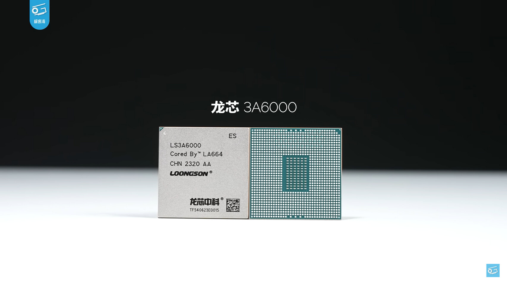
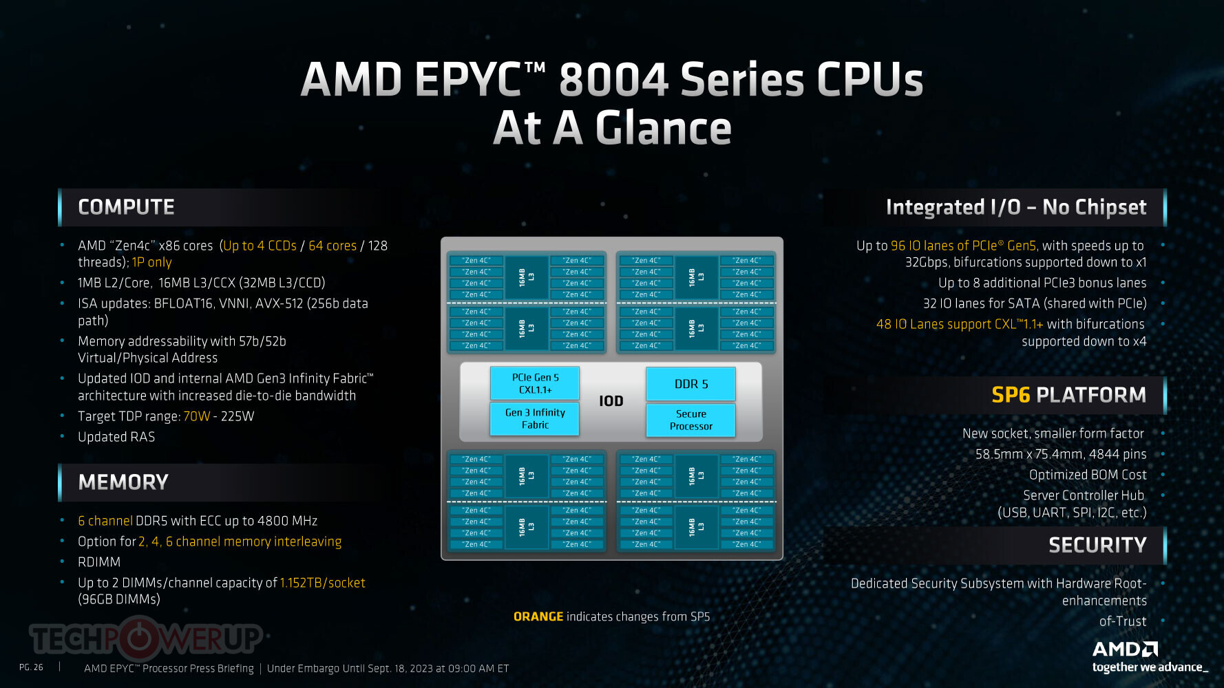
Loongson 3A6000 CPU Reportedly Matches AMD Zen 4 and Intel Raptor Lake IPC

China's homegrown Loongson 3A6000 CPU shows promise but still needs to catch up AMD and Intel's latest offerings in real-world performance. According to benchmarks by Chinese tech reviewer Geekerwan, the 3A6000 has instructions per clock (IPC) on par with AMD's Zen 4 architecture and Intel's Raptor Lake. Using the SPEC CPU 2017 processor benchmark, Geekerwan has clocked all the CPUs at 2.5 GHs to compare the raw benchmark results to Zen 4 and Intel's Raptor Lake (Raptor Cove) processors. As a result, the Loongson 3A6000 seemingly matches the latest designs by AMD and Intel in integer results, with integer IPC measured at 4.8, while Zen 4 and Raptor Cove have 5.0 and 4.9, respectively. The floating point performance is still lagging behind a lot, though. This demonstrates that Loongson's CPU design can catching up to global leaders, but still needs further development, especially for floating point arithmetic.

However, the 3A6000 is held back by low clock speeds and limited core counts. With a maximum boost speed of just 2.5 GHz across four CPU cores, the 3A6000 cannot compete with flagship chips like AMD's 16-core Ryzen 9 7950X running at 5.7 GHz. While the 3A6000's IPC is impressive, its raw computing power is a fraction of that of leading x86 CPUs. Loongson must improve manufacturing process technology to increase clock speeds, core counts, and cache size. The 3A6000's strengths highlight Loongson's ambitions: an in-house LoongArch ISA design fabricated on 12 nm achieves competitive IPC to state-of-the-art x86 chips built on more advanced TSMC 5 nm and Intel 7 nm nodes. This shows the potential behind Loongson's engineering. Reports suggest that next-generation Loongson 3A7000 CPUs will use SMIC 7 nm, allowing higher clocks and more cores to better harness the architecture's potential. So, we expect the next generation to set a bar for China's homegrown CPU performance.

SMIC Reportedly Ramping Up 5 Nanometer Production Line in Shanghai

Semiconductor Manufacturing International Corp (SMIC) is preparing new semiconductor production lines at its Shanghai facilities according to a fresh Reuters report—China's largest contract chip maker is linked to next generation Huawei SoC designs, possibly 5 nm-based Kirin models. SMIC's newest Shanghai wafer fabrication site was an expensive endeavor—involving a $8.8 billion investment—but their flagship lines face a very challenging scenario with new phases of mass production. Huawei, a key customer, is expected to "upgrade" to a 5 nm process for new chip designs—their current flagship, Kirin 9000S, is based on a SMIC 7 nm node. Reuter's industry sources believe that the foundry's current stable of "U.S. and Dutch-made equipment" will be deployed to "produce 5-nanometer chips."

Revised trade rulings have prevented ASML shipping advanced DUV machinery to mainland China manufacturing sites—SMIC workers have reportedly already repurposed the existing inventory of lithography equipment for next-gen pursuits. Burn Lin (ex-TSMC), a renowned "chip guru," believes that it is possible to mass produce 5 nm product on slightly antiquated gear (previously used for 7 nm)—but the main caveats being increased expense and low yields. According to a DigiTimes Asia report, mass production of a 5 nm SoC on SMIC's existing DUV lithography would require four-fold patterning in a best case scenario.

NVIDIA GeForce RTX 4080 SUPER Starts Selling at $999

NVIDIA today launched the third and final high-end GPU in its GeForce RTX 40-series SUPER refresh. The new GeForce RTX 4080 SUPER is being launched at an attractive $999 price, compared to the $1,199 that the RTX 4080 originally launched at. Besides this huge 20% cut in pricing, there's also more performance on offer, as the company chose to max out the 5 nm AD103 silicon that it's based on. If you recall, the RTX 4080 has 76 out of 80 streaming multiprocessors of the AD103 enabled, and its memory runs at an odd 22.4 Gbps speed. The RTX 4080 SUPER gets all 80 SM, and a well rounded 23 Gbps memory speed.

With 80 SM on tap, you get 10,240 CUDA cores, 320 Tensor cores, 80 RT cores, 320 TMUs, and 112 ROPs. The memory size is unchanged at 16 GB, across the 256-bit wide memory interface of the AD103; as is the total graphics power (TGP), at 320 W. All cards will include an NVIDIA-designed adapter that converts three 8-pin PCIe power connectors into a 12VHPWR that's capable of delivering 450 W of power. The target audience for this card is the same as that of the RTX 4080—maxed out 4K Ultra HD gaming with ray tracing. At $999, the RTX 4080 SUPER allows NVIDIA to better compete with the AMD Radeon RX 7900 XTX that's sometimes spotted for prices as low as $900. Don't forget to catch our exhaustive review coverage from the links below!

NVIDIA GeForce RTX 4080 SUPER Founders Edition | ASUS ROG Strix RTX 4080 SUPER OC | ASUS TUF Gaming RTX 4080 SUPER OC | MSI RTX 4080 SUPER Expert | Gigabyte RTX 4080 SUPER Gaming OC | PNY RTX 4080 SUPER Verto | Galax RTX 4080 SUPER SG 1-click OC | Palit RTX 4080 SUPER GamingPro OC | Zotac RTX 4080 SUPER AMP Extreme AIRO

Canon Wants to Challenge ASML with a Cheaper 5 nm Nanoimprint Lithography Machine

Japanese tech giant Canon hopes to shake up the semiconductor manufacturing industry by shipping new low-cost nanoimprint lithography (NIL) machines as early as this year. The technology, which stamps chip designs onto silicon wafers rather than using more complex light-based etching like market leader ASML's systems, could allow Canon to undercut rivals and democratize leading-edge chip production. "We would like to start shipping this year or next year...while the market is hot. It is a very unique technology that will enable cutting-edge chips to be made simply and at a low cost," said Hiroaki Takeishi, head of Canon's industrial group overseeing nanoimprint lithography technological advancement. Nanoimprint machines target a semiconductor node width of 5 nanometers, aiming to reach 2 nm eventually. Takeishi said the technology has primarily resolved previous defect rate issues, but success will depend on convincing customers that integration into existing fabrication plants is worthwhile.

There is skepticism about Canon's ability to significantly disrupt the market led by ASML's expensive but sophisticated extreme ultraviolet (EUV) lithography tools. However, if nanoimprint can increase yields to nearly 90% at lower costs, it could carve out a niche, especially with EUV supply struggling to meet surging demand. Canon's NIL machines are supposedly 40% the cost of ASML machinery, while operating with up to 90% lower power draw. Initially focusing on 3D NAND memory chips rather than complex processors, Canon must contend with export controls limiting sales to China. But with few options left, Takeishi said Canon will "pay careful attention" to sanctions risks. If successfully deployed commercially after 15+ years in development, Canon's nanoimprint technology could shift the competitive landscape by enabling new players to manufacture leading-edge semiconductors at dramatically lower costs. But it remains to be seen whether the new machines' defect rates, integration challenges, and geopolitical headwinds will allow Canon to disrupt the chipmaking giants it aims to compete with significantly.

Intel, Marvell, and Synopsys to Showcase Next-Gen Memory PHY IP Capable of 224 Gbps on 3nm-class FinFET Nodes

The sneak peeks from the upcoming IEEE Solid State Circuit Conference continues, as the agenda items unveil interesting tech that will be either unveiled or demonstrated there. Intel, Synopsys, and Marvell, are leading providers of DRAM physical layer interface (PHY) IP. Various processor, GPU, and SoC manufacturers license PHY and memory controller IP from these companies, to integrate with their designs. All three companies are ready with over 200 Gbps around the 2.69 to 3 petajoule per bit range. This energy cost is as important as the data-rate on offer; as it showcases the viability of the PHY for a specific application (for example, a smartphone SoC has to conduct its memory sub-system at a vastly more constrained energy budget compared to an HPC processor).

Intel is the first in the pack to showcase a 224 Gbps sub-picojoule/bit PHY transmitter that supports PAM4 and PAM6 signaling, and is designed for 3 nm-class FinFET foundry nodes. If you recall, Intel 3 will be the company's final FinFET node before it transitions to nanosheets with the Intel 20A node. At the physical layer, all digital memory signal is analogue, and Intel's IP focuses on the DAC aspect of the PHY. Next up, is a somewhat similar transceiver IP by Synopsys. This too claims 224 Gbps speeds at 3 pJ/b, but at a 40 dB insertion loss; and is designed for 3 nm class FinFET nodes such as the TSMC N3 family and Intel 3. Samsung's 3 nm node uses the incompatible GAAFET technology for its 3 nm EUV node. Lastly, there's Marvell, with a 212 Gb/s DSP-based transceiver for optical direct-detect applications on the 5 nm FinFET nodes, which is relevant for high speed network switching fabrics.

NVIDIA GeForce RTX 4070 Ti SUPER Starts Selling

NVIDIA GeForce RTX 4070 Ti SUPER starts selling today, at a starting price of USD $800. This is the second in a three-part product stack refresh under the SUPER brand extension. This card is designed for maxed out AAA gaming at 1440p, 4K Ultra HD gaming at fairly high settings, 1440p high refresh-rate gaming, as well as gaming in certain ultra-wide resolutions such as 3440 x 1440. The new RTX 4070 Ti SUPER is carved out from the 5 nm AD103 silicon, a physically larger silicon than the AD104 that it had maxed out with the original RTX 4070 Ti. The card enjoys not just a 10% increase in CUDA cores and 20% increase in ROPs, but also a larger 16 GB memory size, across a wider 256-bit memory interface, which is a straight 33% increase in memory bandwidth. The GeForce RTX 4070 Ti SUPER is a partner exclusive launch—there's no Founders Edition card from NVIDIA. Instead, the company ensured that nearly every board partner has cards to offer at the $800 MSRP, with premium overclocked cards being priced in the $850-$900 range.

We have a plethora of RTX 4070 Ti SUPER reviews for you to devour!

ASUS ROG Strix RTX 4070 Ti SUPER OC | ASUS TUF Gaming RTX 4070 Ti SUPER | MSI RTX 4070 Ti SUPER Ventus 3X | Gigabyte RTX 4070 Ti SUPER Gaming OC | Palit RTX 4070 Ti SUPER JetStream OC | PNY RTX 4070 Ti SUPER Verto OC | Gainward RTX 4070 Ti SUPER Phoenix GS | Zotac RTX 4070 Ti SUPER Trinity | Galax RTX 4070 Ti SUPER EX Gamer White

NVIDIA GeForce RTX 4070 SUPER Goes on Sale, Starting at $599

NVIDIA GeForce RTX 4070 SUPER started selling today. The card is generally available, with the NVIDIA MSRP set at USD $599. The RTX 4070 Super is part of a three product refresh of the GeForce RTX 40-series product stack that NVIDIA announced at its 2024 International CES event, on January 8. It offers more performance for the price the RTX 4070 originally sold at, which now comes with a price cut to $549, with its real-world pricing expected to be between $510-560. The RTX 4070 SUPER is based on the same 5 nm "AD104" silicon as the RTX 4070 and RTX 4070 Ti, but comes with a decent bump in shaders over the original RTX 4070.

The GeForce RTX 4070 SUPER is configured with 7,168 CUDA cores—a 21 percent increase over the RTX 4070. It also gets an extra 16 ROPs, maxing out the 80 ROPs present on the silicon. What's more, NVIDIA also unlocked the full 48 MB of on-die L2 cache memory for the RTX 4070 SUPER, which is the same as the RTX 4070 Ti. The original RTX 4070 only has 36 MB of this cache enabled. Spare for 4 SM worth 512 shaders, the RTX 4070 SUPER is almost an RTX 4070 Ti, but there's one last differentiator—power limits. The RTX 4070 SUPER is configured with a total graphics power (TGP) of 220 W, whereas the RTX 4070 Ti has it set at 285 W. Some of the factory-overclocked RTX 4070 SUPER cards attempt to raise this limit by around 20 W. NVIDIA has decided to phase out the RTX 4070 Ti from its product stack, which finds itself replaced with the GeForce RTX 4070 Ti SUPER, coming in next week.

Our extensive Review coverage is as follows: NVIDIA GeForce RTX 4070 SUPER Founders Edition | ASUS TUF Gaming RTX 4070 SUPER OC | Palit RTX 4070 SUPER JetStream | GIGABYTE RTX 4070 SUPER AORUS Master | ZOTAC RTX 4070 SUPER Trinity Black | ASUS RTX 4070 SUPER DUAL | PNY RTX 4070 SUPER Verto | Gainward RTX 4070 SUPER Ghost

NVIDIA Announces the GeForce RTX 40 SUPER Series Graphics Cards

NVIDIA today gave its GeForce RTX 40-series "Ada" a midlife refresh targeting the higher end of its product stack, with the new GeForce RTX 4070 SUPER, GeForce RTX 4070 Ti SUPER, and the GeForce RTX 4080 SUPER. The new RTX 4080 SUPER replaces the current RTX 4080, which will gradually be phased out of the market. The new RTX 4070 Ti SUPER does the same to the current RTX 4070 Ti. The RTX 4070 SUPER, however, will coexist with the current RTX 4070, albeit at a slight price premium. The RTX 4070 SUPER and RTX 4070 Ti SUPER are both being recommended by NVIDIA for maxed out 1440p gaming with full ray tracing; while the RTX 4080 SUPER is for those who want to max out gameplay at 4K with full ray tracing. The RTX 4070 SUPER and RTX 4070 Ti SUPER should still very much be capable of 4K gaming and more than acceptable frame rates, especially given the latest DLSS 3 Frame Generation and its proliferation among new AAA titles.

NVIDIA is giving the three new graphics card SKUs a staggered launch spread across January 2024. The RTX 4070 SUPER should be available to purchase on January 17, at a starting price of $599, which was the original MSRP of the RTX 4070. After this launch, the RTX 4070 slides down a bit to $549 while remaining in the product stack. Things get interesting higher up the stack. The RTX 4070 Ti SUPER, which goes on sale on January 24, is priced at $799, while the current RTX 4070 Ti is being retired from the product stack. The remaining RTX 4070 Ti cards should be up at slightly discounted prices.

Huawei Still Ships 5 nm TSMC Chips in its Laptops, Despite US Sanctions

According to the latest teardown from TechInsights, China's biggest technology maker, Huawei, has been shipping laptops with technology supposedly sanctioned by the United States. As the teardown shows, TechInisights has discovered that Huawei's Kirin 9006C processor is manufactured on TSMC's 5 nm semiconductor technology. Originally, the United States have imposed sanctions on Huawei back in 2020, when the government cut off Huawei's access from TSMC's advanced facilities and forbade the use of the latest nodes by Huawei's HiSilicon chip design arm. Today's findings show signs of contradiction, as the Qingyun L540 notebook that launched in December 2023 employs a Kirin 9006C chipset manufactured on a TSMC 5 nm node.

TechInsight's findings indicate that Kirin 9006C assembly and packaging occurred around the third quarter of 2020, whereas the 2020 Huawei sanctions started in the second quarter. Of course, the implication of the sanctions likely prohibited any new orders and didn't prevent Huawei from possibly stockpiling millions of chip orders in its warehouse before they took place. The Chinese giant probably made orders beforehand and is using the technology only now, with the Qingyun L540 laptop being one of the first Kirin 9006C appearances. Some online retailers also point out that the laptop complies with the latest security practices required for the government, which means that they have been in the works since the chip began the early stages of design, way before 2020. We don't know the stockpile quantity, but SMIC's domestic efforts seem insufficient to supply the Chinese market alone. The news that Huawei is still using TSMC chips made SMIC's share go for a 2% free fall on the Hong Kong stock exchange.

DEEPX's DX-M1 Chip Recognized at CES 2024 as Leading AI of Things Solution

DEEPX (CEO, Lokwon Kim), an original AI semiconductor technology company, is announcing that it has surpassed 40 customers for its flagship chip solution, DX-M1—the only AI accelerator on the market to combine low power consumption, high efficiency and performance, and cost-effectiveness. The groundbreaking solution has been deployed for a hands-on trial to this customer pool, which spans global companies and domestic Korean enterprises across various sectors.

DEEPX is currently running an Early Engagement Customer Program (EECP) to provide customers with early access to its small camera module, a one-chip solution featuring DX-V1; M.2 module featuring DX-M1; and DXNN, the company's developer environment. This allows customers to receive pre-production validation of DEEPX's hardware and software, integrate them into mass-produced products, and realize AI technology innovations with the brand's technical support.

AMD Close to Launching Radeon RX 7800M Series Based on "Navi 32"

AMD's small Radeon RX 7000M and RX 7000S lines of mobile GPUs based on the latest RDNA 3 graphics architecture includes just five SKUs, spanning the "Navi 31" and "Navi 33" chips. The RX 7000M series only has enthusiast-segment RX 7900M series based on the "Navi 31," and the RX 7600M series based on the "Navi 33," leaving a vast gap that the company plans to fill with RX 7800M series and RX 7700M series SKUs based on the "Navi 32," referred to internally as "Cuarzo Verde." The GPU is meant to be hardwired onto the mainboards of gaming notebooks, however, AMD hands out reference-design MXM boards to OEMs. These were sniffed out in a public shipping manifest harukaze5719 on Twitter.

The "Navi 32" package is roughly similar in size to the compacted "Navi 31" package powering the RX 7900M series. It has a physically smaller 5 nm GCD with 60 compute units compared to the 96 on the "Navi 31" GCD; and is surrounded by four 6 nm MCDs, which give it 64 MB of Infinity Cache, and a 256-bit GDDR6 memory bus. With this, AMD has the option of not just carving out RX 7800M series and RX 7700M series SKUs, but also RX 7900S series SKUs within its segment aimed at gaming-grade ultraportables. We could see some product announcements to this effect Q1 2024, alongside some new desktop SKUs.

ASUS Intros China-exclusive Radeon RX 7900 GRE TUF White

ASUS over the weekend introduced the China-exclusive Radeon RX 7900 GRE TUF Gaming White graphics card. The card shares a lot in common with the other RX 7900 series TUF Gaming custom-design cards, but swaps out the gunmetal-gray cooler shroud and backplate combo for one that's matte white. The whitewash even extends to the impellers of the three Axial Tech fans. The PCB remains black, but due to the 3-D design of the shroud and backplate, is largely concealed. The card draws power from a pair of 8-pin PCIe power connectors, and uses a 14-phase VRM to condition it for the "Navi 31 XL" ASIC.

The Radeon RX 7900 GRE (golden rabbit edition) is based on a "Navi 31 XL," a unique package that combines the 5 nm graphics compute die (GCD) of "Navi 31," with the 4-MCD (memory cache die) setup of the smaller "Navi 32" package. AMD designed this primarily to drive the mobile RX 7900 series SKUs, but it found its way to the desktop platform to fill the gap between the RX 7800 XT and RX 7900 XT, and possibly undercut the GeForce RTX 4070 Ti. It is configured with 80 out of 96 available compute units on the GCD, giving it 5,120 stream processors, 160 AI accelerators, and 80 Ray accelerators, the Infinity Cache size is reduced to 64 MB, since there are only 4 MCDs, driving its 256-bit memory bus that handles 16 GB of 18 Gbps GDDR6 memory (576 GB/s bandwidth).

Two New Marvell OCTEON 10 Processors Bring Server-Class Performance to Networking Devices

Marvell Technology, a leader in data infrastructure semiconductor solutions, is enabling networking equipment and firewall manufacturers achieve breakthrough levels of performance and efficiency with two new OCTEON 10 data processing units (DPUs), the OCTEON 10 CN102 and OCTEON 10 CN103. The 5 nm OCTEON CN102 and CN103, broadly available to OEMs for product design and pilot production, are optimized for data and control plane applications in routers, firewalls, 5G small cells, SD-WAN appliances, and control plane applications in top-of-rack switches and line card controllers. Several of the world's largest networking equipment manufacturers have already incorporated the OCTEON 10 CN102 into a number of product designs.

Containing up to eight Arm Neoverse N2 cores, OCTEON 10 CN102 and CN103 deliver 3x the performance of Marvell current DPU solutions for devices while reducing power consumption by 50% to 25 W. Achieving SPEC CPU (2017) integer rate (SPECint) scores of 36.5, OCTEON 10 CN102 and CN103 are able to deliver nearly 1.5 SPECint points per Watt. The chips can serve as an offload DPU for host processors or as the primary processor in devices; advanced performance per watt also enables OEMs to design fanless systems to simplify systems and further reduce cost, maintenance and power consumption.

Top 10 Foundries Experience 7.9% QoQ Growth in 3Q23, with a Continued Upward Trend Predicted for Q4

TrendForce's research indicates a dynamic third quarter for the global foundry industry, marked by an uptick in urgent orders for smartphone and notebook components. This surge was fueled by healthy inventory levels and the release of new iPhone and Android devices in 2H23. Despite persisting inflation risks and market uncertainties, these orders were predominantly executed as rush orders. Additionally, TSMC and Samsung's high-cost 3 nm manufacturing process had a positive impact on revenues, driving the 3Q23 value of the top ten global foundries to approximately US$28.29 billion—a 7.9% QoQ increase.

Looking ahead to 4Q23, the anticipation of year-end festive demand is expected to sustain the inflow of urgent orders for smartphones and laptops, particularly for smartphone components. Although the end-user market is yet to fully recover, pre-sales season stockpiling for Chinese Android smartphones appears to be slightly better than expected, with demand for mid-to-low range 5G and 4G phone APs and continued interest in new iPhone models. This scenario suggests a continued upward trend for the top ten global foundries in Q4, potentially exceeding the growth rate seen in Q3.

Microsoft Introduces 128-Core Arm CPU for Cloud and Custom AI Accelerator

During its Ignite conference, Microsoft introduced a duo of custom-designed silicon made to accelerate AI and excel in cloud workloads. First of the two is Microsoft's Azure Cobalt 100 CPU, a 128-core design that features a 64-bit Armv9 instruction set, implemented in a cloud-native design that is set to become a part of Microsoft's offerings. While there aren't many details regarding the configuration, the company claims that the performance target is up to 40% when compared to the current generation of Arm servers running on Azure cloud. The SoC has used Arm's Neoverse CSS platform customized for Microsoft, with presumably Arm Neoverse N2 cores.

The next and hottest topic in the server space is AI acceleration, which is needed for running today's large language models. Microsoft hosts OpenAI's ChatGPT, Microsoft's Copilot, and many other AI services. To help make them run as fast as possible, Microsoft's project Athena now has the name of Maia 100 AI accelerator, which is manufactured on TSMC's 5 nm process. It features 105 billion transistors and supports various MX data formats, even those smaller than 8-bit bit, for maximum performance. Currently tested on GPT 3.5 Turbo, we have yet to see performance figures and comparisons with competing hardware from NVIDIA, like H100/H200 and AMD, with MI300X. The Maia 100 has an aggregate bandwidth of 4.8 Terabits per accelerator, which uses a custom Ethernet-based networking protocol for scaling. These chips are expected to appear in Microsoft data centers early next year, and we hope to get some performance numbers soon.

AMD Announces Ryzen Embedded 7000 Series Processors Powered by Zen 4

AMD today announced at Smart Production Solutions 2023 the AMD Ryzen Embedded 7000 Series processor family, optimized for the high-performance requirements of industrial markets. By combining "Zen 4" architecture and integrated Radeon graphics, Ryzen Embedded 7000 Series processors deliver performance and functionality not previously offered for the embedded market. With its expanded features and integration, Ryzen Embedded 7000 Series processors are ideal for a wide range of embedded applications, including industrial automation, machine vision, robotics and edge servers.

The Ryzen Embedded 7000 Series processor is the first embedded processor to use next-generation 5 nm technology with a 7-year manufacturing availability commitment. The new embedded processor integrates AMD Radeon RDNA 2 graphics that eliminates the need for a discrete GPU for industrial applications. And because embedded applications require additional operating system software options, Ryzen Embedded 7000 Series processors include support for both Windows Server and Linux Ubuntu, on top of Windows 10 and Windows 11. Ryzen Embedded 7000 Series processors also include up to 12 high-performance "Zen 4" CPU cores, which combined with its integrated features and wide operating system choices, offers unparalleled ease of integration for system designers.

AMD Mobile Processor Lineup in 2025 Sees "Fire Range," "Strix Halo," and Signficant AI Performance Increases

With Windows 11 23H2 setting the stage for increased prevalence of AI in client PC use cases, the new hardware battleground between AMD and its rivals Intel, Apple, and Qualcomm, will be in equipping their mobile processors with sufficient AI acceleration performance. AMD already introduced accelerated AI with the current "Phoenix" processor that debuts Ryzen AI, and its Xilinx XDNA hardware backend that provides a performance of up to 16 TOPS. This will see a 2-3 fold increase with the company's 2024-25 mobile processor lineup, according to a roadmap leak by "Moore's Law is Dead."

At the very top of the pile, in a product segment called "ultimate compute," which consists of large gaming notebooks, mobile workstations, and desktop-replacements; the company's current Ryzen 7045 "Dragon Range" processor will continue throughout 2024. Essentially a non-socketed version of the desktop "Raphael" MCM, "Dragon Range" features up to two 5 nm "Zen 4" CCDs for up to 16 cores, and a 6 nm cIOD. This processor lacks any form of AI acceleration. In 2025, the processor will be succeeded with "Fire Range," a similar non-socketed, mobile-friendly MCM that's derived from "Granite Ridge," with up to two 4 nm "Zen 5" CCDs for up to 16 cores; and the 6 nm cIOD. What's interesting to note here, is that the quasi-roadmap makes no mention of AI acceleration for "Fire Range," which means "Granite Ridge" could miss out on Ryzen AI acceleration from the processor. Modern discrete GPUs from both NVIDIA and AMD support AI accelerators, so this must have been AMD's consideration to exclude an XDNA-based Ryzen AI accelerator on "Fire Range" and "Granite Ridge."

US Government Can't Stop Chinese Semiconductor Advancement, Notes Former TSMC VP

The Chinese semiconductor industry is advancing, and interestingly, it is growing rapidly under sanctions, even with the blacklisting of companies by the US government. China's semiconductor industry is mainly represented by companies like Semiconductor Manufacturing International Corp (SMIC) and Huawei Technologies, who are leading the investment and progress in both chip manufacturing and chip design. According to the latest interview with Bloomberg, former TSMC Vice President Burn J. Lin said that the US government and its sanctions can not stop the advancement of Chinese semiconductor companies. Currently, Lin notes that SMIC and Huawei can use older machinery to produce more advanced chips.

Even so, SMIC could progress to 5 nm technology using existing equipment, particularly with scanners and other machinery from ASML. Development under sanctions would also force China to experiment with new materials and other chip packaging techniques that yield higher performance targets. SMIC has already developed a 7 nm semiconductor manufacturing node, which Huawei used for its latest Mate 60 Pro smartphone, based on Huawei's custom HiSilicon Kirin 9000S chip. Similarly, the transition is expected to happen to the 5 nm node as well, and it is only a matter of time before we see other nodes appear. "It is just not possible for the US to completely prevent China from improving its chip technology," noted Burn J. Lin.

Tachyum Books Purchase Order to Build System with 25,000x ChatGPT4 Capacity and 25x Faster than Current Supercomputers

Tachyum announced that it has accepted a major purchase order from a US company to build a large-scale system, based on its 5 nm Prodigy Universal Processor chip, which delivers more than 50 exaflops performance that will exponentially exceed the computational capabilities of the fastest inference or generative AI supercomputers available anywhere in the world today.

Prodigy, the world's first Universal Processor, is engineered to transform the capacity, efficiency and economics of datacenters through its industry-leading performance for hyperscale, high-performance computing and AI workloads. When complete, the Prodigy-powered system will deliver a 25x multiplier vs. the world's fastest conventional supercomputer built just this year, and will achieve AI capabilities 25,000x larger than models for ChatGPT4.

AMD EPYC 8004 "Siena" Processors with "Zen 4c" and New SP6 Platform Announced

AMD today rolled out the new compacted Socket SP6 server platform designed for smaller servers locally deployed at the edge by organizations. With CPU core-counts of up to 64-core/128-thread, these processors are based on the "Zen 4c" microarchitecture, which comes with identical IPC and ISA to "Zen 4," but with smaller L3 cache available per core. The EPYC 8004 series targets traditional data-centers located on-site for organizations. Even if the heavy-lifting of the IT for them is performed by remote data-centers or cloud providers, organizations still need smaller edge server deployments. The EPYC 8004 series caters to a different kind of servers than the ones the lower core-count models of EPYC 9004 "Genoa" do.

With the EPYC 8004 series, AMD is debuting a new smaller CPU socket called SP6. The socket measures 58.5 mm x 75.4 mm, compared to the 76.0 mm x 80.0 mm of Socket SP5 powering EPYC 9004 "Genoa" and EPYC 97x4 "Bergamo." Socket SP5 is an LGA with a pin count of 4,844, compared to SP5, which is LGA-6096. The first line of processors for this socket, the EPYC 8004 series, are codenamed "Siena." These are very much part of the 4th Gen EPYC series, a lineage it shares with "Genoa" for data-center servers, "Genoa-X" for compute servers, and "Bergamo" for high-density cloud.

Intel Foundry Services and Tower Semiconductor Announce New US Foundry Agreement

Intel Foundry Services (IFS) and Tower Semiconductor, a leading foundry for analog semiconductor solutions, today announced an agreement where Intel will provide foundry services and 300 mm manufacturing capacity to help Tower serve its customers globally. Under the agreement, Tower will utilize Intel's advanced manufacturing facility in New Mexico. Tower will invest up to $300 million to acquire and own equipment and other fixed assets to be installed in the New Mexico facility, providing a new capacity corridor of over 600,000 photo layers per month for Tower's future growth, enabling capacity to support forecasted customer demand for 300 mm advanced analog processing.

This agreement demonstrates the commitment from both Intel and Tower to expand their respective foundry footprints with unparalleled solutions and scaled capabilities. Intel will manufacture Tower's highly differentiated 65-nanometer power management BCD (bipolar-CMOS-DMOS) flows, among other flows at Intel's Fab 11X in Rio Rancho, New Mexico.

Top Ten Semiconductor Foundries Report a 1.1% Quarterly Revenue Decline in 2Q23, Anticipated to Rebound in 3Q23

TrendForce reports an interesting shift in the electronics landscape: dwindling inventories for TV components, along with a surging mobile repair market that's been driving TDDI demand, have sparked a smattering of urgent orders in the Q2 supply chain. These last-minute orders have served as pivotal lifelines, propping up Q2 capacity utilization and revenue for semiconductor foundries. However, the adrenaline rush from these stop-gap orders may be a short-lived phenomenon and is unlikely to be carried over into the third quarter.

On the other hand, demand for staple consumer products like smartphones, PCs, and notebooks remains sluggish, perpetuating a slump in the use of expensive, cutting-edge manufacturing processes. At the same time, traditionally stable sectors—automotive, industrial control, and servers—are undergoing inventory correction. The confluence of these trends has resulted in a sustained contraction for the world's top ten semiconductor foundries. Their global revenue declined by approximately 1.1% for the quarter, amounting to a staggering US$26.2 billion.

AMD Unveils Radeon RX 7800 XT and RX 7700 XT Graphics Cards

AMD today at Gamescom unveiled the Radeon RX 7800 XT and Radeon RX 7700 XT performance-segment graphics cards. Designed for maxed out gaming at 1440p with ray tracing, the two are designed to square off against NVIDIA's GeForce RTX 4070 series, offering competitive performance and pricing. The two are based on AMD's latest RDNA3 graphics architecture, and use the 5 nm foundry process where it matters. Both cards claim to offer not just superior performance to the specific NVIDIA RTX 40-series SKUs they're designed to compete with, but also better future-proofing, with more video memory on offer.

At the heart of the two is the new "Navi 32" GPU, AMD's second largest chip from this generation. It is a chiplet GPU, just like the "Navi 31" that powers the RX 7900 series, albeit slightly scaled down. The graphics compute die (GCD), the die with the main graphics rendering and compute machinery, is built on the 5 nm EUV foundry node. It is flanked by four memory cache dies (MCDs), each built on the 6 nm foundry node. These are the same MCDs found in the "Navi 31," but four in number instead of six, which gives the "Navi 32" a 256-bit wide GDDR6 memory interface.

AMD "Navi 4C" GPU Detailed: Shader Engines are their own Chiplets

"Navi 4C" is a future high-end GPU from AMD that will likely not see the light of day, as the company is pivoting away from the high-end GPU segment with its next RDNA4 generation. For AMD to continue investing in the development of this GPU, the gaming graphics card segment should have posted better sales, especially in the high-end, which it didn't. Moore's Law is Dead scored details of what could have been a fascinating technological endeavor for AMD, in building a highly disaggregated GPU.

AMD's current "Navi 31" GPU sees a disaggregation of the main logic components of the GPU that benefit from the latest 5 nm foundry node to be located in a central Graphics Compute Die; surrounded by up to six little chiplets built on the older 6 nm foundry node, which contain segments of the GPU's Infinity Cache memory, and its memory interface—hence the name memory cache die. With "Navi 4C," AMD had intended to further disaggregate the GPU, identifying even more components on the GCD that can be spun out into chiplets; as well as breaking up the shader engines themselves into smaller self-contained chiplets (smaller dies == greater yields and lower foundry costs).

AMD Radeon RX 7700 XT Confirmed with 192-bit Memory Bus in ASRock Regulatory Leak

AMD Radeon RX 7700 XT is confirmed to feature 12 GB as its standard memory size, and feature a 192-bit wide GDDR6 memory interface, according to a leaked regulatory filing by ASRock for its upcoming graphics cards. We already know from last week's mega leak of the PowerColor RX 7800 XT Red Devil that the card maxes out the "Navi 32" silicon, enabling all 60 RDNA3 CU, and comes with 16 GB of memory across the chip's full 256-bit memory bus. This filing suggests how AMD will carve the RX 7700 XT out.

Probably designed to compete with the GeForce RTX 4070, the RX 7700 XT is based on the same "Navi 32" silicon as the RX 7800 XT, but cut down. AMD is expected to disable some of the 60 CU physically present on the 5 nm GCD, while one of the four 6 nm MCDs will be disabled, giving the chip a 192-bit memory bus to drive its 12 GB of memory. We know from the PowerColor leak that the RX 7800 XT gets 18 Gbps memory speed. It remains to be seen if AMD sticks with this speed for even the RX 7700 XT, in which case, it gets 432 GB/s of memory bandwidth at its disposal. AMD is expected to launch the RX 7800 XT and RX 7700 XT within this quarter (before October).
Return to Keyword Browsing
Jul 15th, 2025 19:48 CDT change timezone

New Forum Posts

Popular Reviews

TPU on YouTube

Controversial News Posts