News Posts matching #5 nm

Return to Keyword Browsing

TSMC 3 nm To Enter Volume Production in 2022

TSMC will commercialize its N3 (3 nm) EUV silicon fabrication node in 2022, with volume production set to commence in the second half of the year. The company is looking to maximize capacity on its current N5 (5 nm) node, which already serves major customers such as Apple. AMD is expected to utilize N5 allocation going into 2022 as its next-generation "Zen 4" processors are expected to leverage the node to drive up CPU core counts and caches. The company is also utilizing N6 (6 nm) for its CDNA2 compute accelerator logic dies. N5 could also power mobile application processors from several manufacturers.

TSMC Expands Advanced Technology Leadership with N4P Process

TSMC today introduced its N4P process, a performance-focused enhancement of the 5-nanometer technology platform. N4P joins the industry's most advanced and extensive portfolio of leading-edge technology processes. With N5, N4, N3 and the latest addition of N4P, TSMC customers will have multiple and compelling choices for power, performance, area, and cost for its products.

As the third major enhancement of TSMC's 5 nm family, N4P will deliver an 11% performance boost over the original N5 technology and a 6% boost over N4. Compared to N5, N4P will also deliver a 22% improvement in power efficiency as well as a 6% improvement in transistor density. In addition, N4P lowers process complexity and improves wafer cycle time by reducing the number of masks. N4P demonstrates TSMC's pursuit and investment in continuous improvement of our process technologies.

Alibaba Goes Anti-x86: Open-Source RISC-V and 128-Core Arm Server Processors on the Horizon

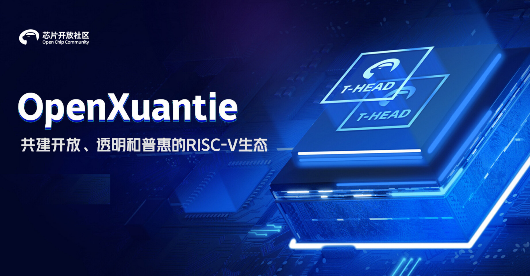
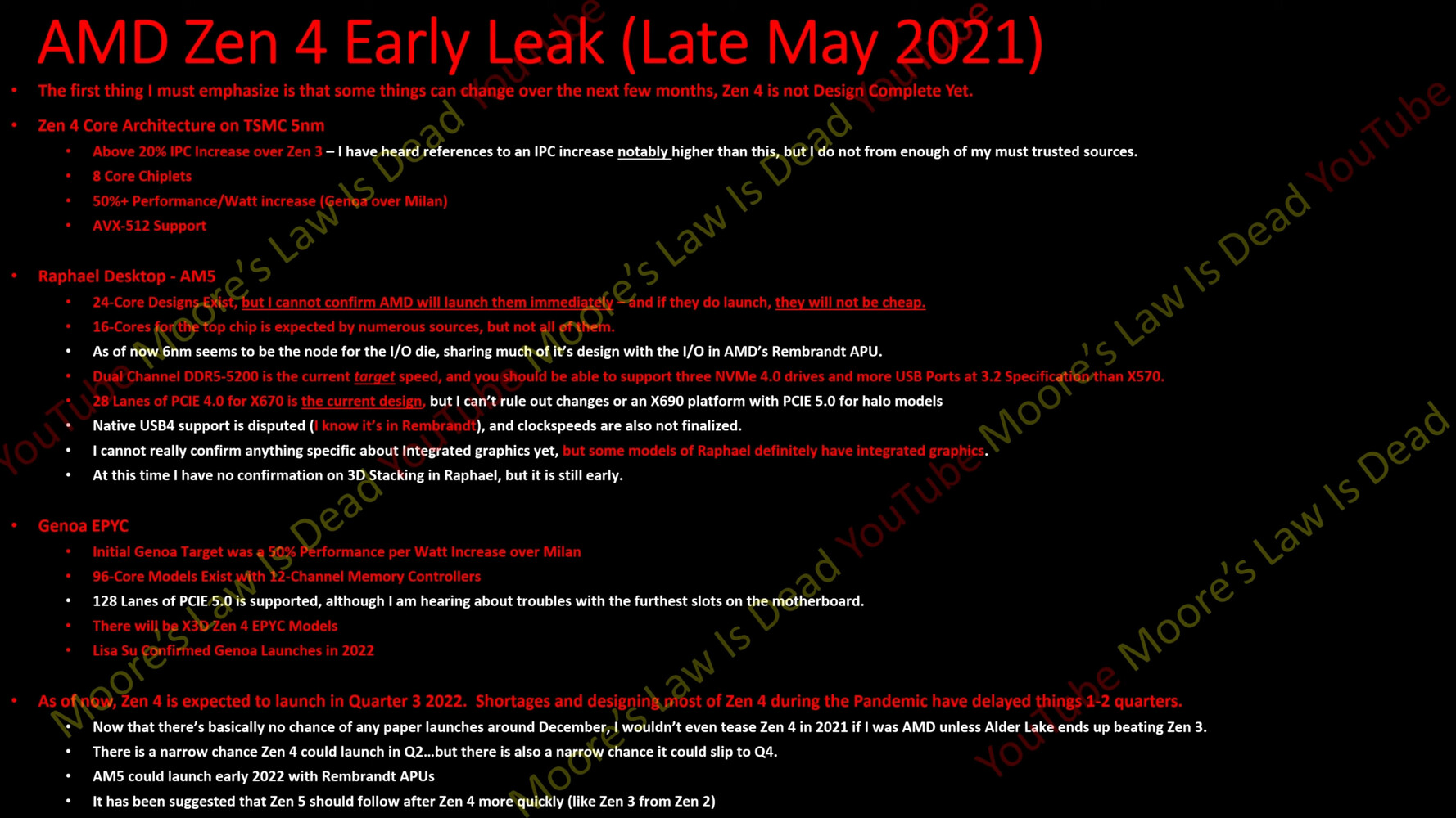
With the x86 architecture, large hyperscale cloud providers have been experiencing all sorts of troubles, from high power consumption to the high pricing structure of these processors. Companies like Amazon Web Services (AWS) build their processors based on 3rd party instruction set architecture designs. Today, Alibaba, the Chinese giant, has announced the launch of two processors made in-house to serve everything from edge to central server processing. First in line is the RISC-V-based Xuantie series of processors, which can run anything from AliOS, FreeRTOS, RT-Thread, Linux, Android, etc., to other operating systems as well. These processors are open-source, capable of modest processing capabilities, and designed as IPs that anyone can use. You can check them out on T-Head GitHub repositories here.

The other thing that Alibaba announced is the development of a 128-core custom processor based on the Arm architecture. Called Yitian 710 server SoC, TSMC manufactures it on the company on 5 nm semiconductor node. So far, Alibaba didn't reveal any details about the SoC and what Arm cores are used. However, this signifies that the company seeks technology independence from outside sources and wants to take it all in-house. With custom RISC-V processors for lower-power tasks and custom Arm server CPUs, the whole infrastructure is covered. It is just a matter of time before Alibaba starts to replace x86 makers in full. However, given the significant number of chips that the company needs, it may not happen at any sooner date.

Marvell Expands 5nm Data Infrastructure Portfolio with New Prestera Carrier Switch and OCTEON 10 DPU

Marvell today announced the expansion of its industry-leading 5 nm data infrastructure platform with the launch of the industry's first 5 nm 50G PAM4 device for the carrier market, the Prestera DX 7321 Ethernet switch. The new switch builds on the success of the Prestera carrier-optimized portfolio and is ideal for 5G fronthaul and edge connectivity. In concert with this, Marvell's 5 nm OCTEON 10 DPU family, incorporating industry-leading hardware accelerators, is now sampling. By utilizing the industry's leading advanced process geometry, the Marvell Prestera switch and OCTEON DPU deliver 50% lower power than existing offerings, enabling new infrastructure solutions for next-generation carrier edge networks and RAN deployment models.

With the addition of the 5 nm Prestera device, the expanded carrier-optimized switch portfolio now comprises four cutting-edge Ethernet switches that scale port speeds from 1 Gbps to 400 Gbps with aggregate bandwidths ranging from 200 Gbps to 1.6 Tbps. The newest offering enhances Marvell's 5G solutions for Open RAN, vRAN and traditional RAN architectures, with Class D precision time protocol (PTP), which provides more timing headroom to enable larger cell coverage radius. The switch device incorporates integrated MACsec security and advanced telemetry to facilitate network visibility and automation.

Samsung Foundry Announces GAA Ready, 3nm in 2022, 2nm in 2025, Other Speciality Nodes

Samsung Electronics, a world leader in advanced semiconductor technology, today unveiled plans for continuous process technology migration to 3- and 2-nanometer (nm) based on the company's Gate-All-Around (GAA) transistor structure at its 5th annual Samsung Foundry Forum (SFF) 2021. With a theme of "Adding One More Dimension," the multi-day virtual event is expected to draw over 2,000 global customers and partners. At this year's event, Samsung will share its vision to bolster its leadership in the rapidly evolving foundry market by taking each respective part of foundry business to the next level: process technology, manufacturing operations, and foundry services.

"We will increase our overall production capacity and lead the most advanced technologies while taking silicon scaling a step further and continuing technological innovation by application," said Dr. Siyoung Choi, President and Head of Foundry Business at Samsung Electronics. "Amid further digitalization prompted by the COVID-19 pandemic, our customers and partners will discover the limitless potential of silicon implementation for delivering the right technology at the right time."

NVIDIA Rumored to Refresh RTX 30-series with SUPER SKUs in January, RTX 40-series in Q4-2022

NVIDIA is rumored to be giving its GeForce RTX 30-series "Ampere" graphics card family a mid-term refresh by the 2022 International CES, in January; the company is also targeting Q4-2022, specifically October, to debut its next-generation RTX 40-series. The Q1 refresh will include "SUPER" branded SKUs taking over key price-points for NVIDIA, as it lands up with enough silicon that can be fully unlocked. This leak comes from Greymon55, a reliable source on NVIDIA leaks. It also aligns with the most recent pattern followed by NVIDIA to keep its GeForce product-stack updated. The company had recently released "Ti" updates to certain higher-end price-points, in response to competition from the Radeon RX 6000 "RDNA2" series.

NVIDIA's next-generation will be powered by the "Lovelace" graphics architecture that sees even more hardware acceleration for the RTX feature-set, more raytraced effects, and preparation for future APIs. It also marks NVIDIA's return to TSMC, with the architecture reportedly being designed for the 5 nm (N5) silicon fabrication node. The current-gen GeForce "Ampere" chips are being products on an 8 nm foundry node by Samsung.

Samsung Receives its First Global Carbon Footprint Certification for Logic Chips

Samsung Electronics Co., Ltd., a world leader in advanced semiconductor technology, today announced that four of its System LSI products received product carbon footprint label certification from the Carbon Trust, the first of Samsung's logic chips to do so. Having received the semiconductor industry's first carbon footprint accreditation for memory chips from the Carbon Trust in 2019, Samsung has now broadened its ESG (Environmental, Social, and Governance) spectrum with this global recognition of 'eco-friendly' logic chips. Samsung also grabbed the industry's first triple Carbon Trust Standard for Carbon, Water and Waste in June 2021.

The Carbon Trust is an independent and expert partner of organizations around the world that advises businesses on their opportunities in a sustainable, low carbon world. The Carbon Trust also measures and certifies the environmental footprint of organizations, supply chains and products. Of the various certification categories of the Carbon Trust, Samsung's System LSI products received the CO2 Measured product carbon footprint label. The label certifies the chip's carbon footprint, which informs consumers of the impact that the product and its manufacturing process have on the environment. Receiving the CO₂ Measured label is a critical first step for carbon reduction, since it verifies the current carbon emissions of the product with globally recognized specifications (PAS 2050), which Samsung can use as a benchmark to measure future carbon reductions.

AMD Socket AM5 "Zen 4" Processors to have RDNA2 Integrated Graphics Across the Lineup

The first desktop processors to implement AMD's "Zen 4" microarchitecture will feature integrated graphics as standard across the lineup, according to a Chips and Cheese report citing leaked AMD design documents. Currently, most of the Socket AM4 desktop processor lineup lacks integrated graphics, and specialized "G" SKUs with integrated graphics dot it. These SKUs almost always come with compromises in CPU performance or PCIe I/O. With its 5 nm "Raphael" Socket AM5 desktop processor, AMD is planning to change this, in a bid to match up to Intel on the universality of integrated graphics.

Built in the 5 nm silicon fabrication process, the "Raphael" silicon combines "Zen 4" CPU cores along with an iGPU based on the RDNA2 graphics architecture. This would be the first time AMD updated the SIMD architecture of its Ryzen iGPUs since 2017. The RDNA2-based iGPU will come with a more advanced DCN (Display CoreNext) component than current RDNA2-based discrete GPUs, with some SKUs even featuring DisplayPort 2.0 support, besides HDMI 2.1. By the time "Raphael" is out (2022-23), it is expected that USB4 type-C would gain popularity, and mainstream motherboards as well as pre-built desktops could ship with USB4 with DisplayPort 2.0 passthrough. AMD relies on a discrete USB4 controller with PCI-Express 4.0 x4 wiring, for its first Socket AM5 platform.

AMD Radeon RX 7000 Series to Include 6nm Optical-Shrinks of RDNA2

AMD's upcoming Radeon RX 7000 series could include GPUs from both the RDNA3 and RDNA2 graphics architectures, according to reliable sources on social media. This theory holds that the company could introduce new 5 nm GPUs based on the new RDNA3 architecture for the higher end, namely the Navi 31 and Navi 32; while giving the current-gen RDNA2 architecture a new lease of life in the lower segments. This isn't, however, a simple rebrand.

Apparently, some existing Navi 2x series chips will receive an optical shrink to the 6 nm node, in a bid to improve their performance/Watt. Some of the performance/Watt improvement could be used to increase engine clocks. These include the Navi 22, with its 40 RDNA2 compute units and 192-bit GDDR6 memory bus; and the Navi 23, with its 32 RDNA2 compute units and 128-bit GDDR6 memory bus. The updated Navi 22 will power the SKU that succeeds the current RX 6600 XT, while the updated Navi 23 works the lower-mainstream SKU RX x500-class.

Penetration Rate of Ice Lake CPUs in Server Market Expected to Surpass 30% by Year's End as x86 Architecture Remains Dominant, Says TrendForce

While the server industry transitions to the latest generation of processors based on the x86 platform, the Intel Ice Lake and AMD Milan CPUs entered mass production earlier this year and were shipped to certain customers, such as North American CSPs and telecommunication companies, at a low volume in 1Q21, according to TrendForce's latest investigations. These processors are expected to begin seeing widespread adoption in the server market in 3Q21. TrendForce believes that Ice Lake represents a step-up in computing performance from the previous generation due to its higher scalability and support for more memory channels. On the other hand, the new normal that emerged in the post-pandemic era is expected to drive clients in the server sector to partially migrate to the Ice Lake platform, whose share in the server market is expected to surpass 30% in 4Q21.

Next-Gen AMD Radeon RDNA3 Flagship To Feature 15,360 Stream Processors?

AMD's next generation RDNA3 graphics architecture generation could see a near-quadrupling in raw SIMD muscle over the current RDNA2, according to a spectacular rumor. Apparently, the company will deploy as many as 15,360 stream processors (quadruple that of a Radeon RX 6800), and spread across 60 WGPs (Workgroup Processors), and do away with the compute unit. This is possibly because the RDNA3 compute unit won't be as independent as the ones on the original RDNA or even RDNA2, which begins to see groups of two CUs share common resources.

Another set of rumors suggest that AMD won't play NVIDIA's game of designing GPUs with wide memory bus widths, and instead build on its Infinity Cache technology, by increasing the on-die cache size and bandwidth, while retaining "affordable" discrete memory bus widths, such as 256-bit. As for the chip itself, it's rumored that the top RDNA3 part, the so-called "Navi 31," could feature a multi-chip module design (at least two logic dies), each with 30 WGPs. Each of the two is expected to be built on a next-gen silicon fabrication node that's either TSMC N5 (5 nm), or a special 6 nm node TSMC is designing for AMD. Much like the next-generation "Lovelace" architecture by NVIDIA, AMD's RDNA3 could see the light of the day only in 2022.

NVIDIA "Ada Lovelace" Architecture Designed for N5, GeForce Returns to TSMC

NVIDIA's upcoming "Ada Lovelace" architecture, both for compute and graphics, is reportedly being designed for the 5 nanometer silicon fabrication node by TSMC. This marks NVIDIA's return to the Taiwanese foundry after its brief excursion to Samsung, with the 8 nm "Ampere" graphics architecture. "Ampere" compute dies continue to be built on TSMC 7 nm nodes. NVIDIA is looking to double the compute performance on its next-generation GPUs, with throughput approaching 70 TFLOP/s, from a numeric near-doubling in CUDA cores, generation-over-generation. These will also be run at clock speeds above 2 GHz. One can expect "Ada Lovelace" only by 2022, as TSMC N5 matures.

Samsung 5 nm Node Struggles With Yields, Reports Indicate Less Than 50% Yielding

Semiconductor manufacturing is no easy task. Every company in that business knows that, and the hardships of silicon manufacturing have been felt by even the greatest players like Samsung and Intel. Today, according to the latest report from Business Korea, Samsung is again in trouble with its 5 nm node. It has been reported previously that Samsung is struggling with yields of its 5 nm node, however, we didn't know just how much until now. According to the sources over at Business Korea, Samsung's 5 nm semiconductor node is experiencing less than 50% yields. That means, for example, that out of 100 chips manufactured on a single silicon wafer, only half are functional. And that is not good at all.

Usually, for a node to go into high-volume manufacturing (HVM), the yielding rate needs to be around 95%. In case it is not at that level, manufacturing of that node is not very efficient and not very profitable. The V1 Line in Hwaseong, where this Samsung 5 nm is made, uses EUV tools to manufacture the new node. While the yields are currently below 50%, it is expected to improve as Samsung engineers tweak and tune the node and the tools that are running the facility. We can expect to hear more about the yields of this node in the coming months.

Intel Ponte Vecchio GPU to Be Liquid Cooled Inside OAM Form Factor

Intel's upcoming Ponte Vecchio graphics card is set to be the company's most powerful processor ever designed, and the chip is indeed looking like an engineering marvel. From Intel's previous teasers, we have learned that Ponte Vecchio is built using 47 "magical tiles" or 47 dies which are responsible either for computing elements, Rambo Cache, Xe links, or something else. Today, we are getting a new piece of information coming from Igor's LAB, regarding the Ponte Vecchio and some of its design choices. For starters, the GPU will be a heterogeneous design that consists out of many different nodes. Some parts of the GPU will be manufactured on Intel's 10 nm SuperFin and 7 nm technologies, while others will use TSMC's 7 nm and 5 nm nodes. The smaller and more efficient nodes will probably be used for computing elements. Everything will be held together by Intel's EMIB and Foveros 3D packaging.

Next up, we have information that this massive Intel processor will be accountable for around 600 Watts of heat output, which is a lot to cool. That is why in the leaked renders, we see that Intel envisioned these processors to be liquid-cooled, which would make the cooling much easier and much more efficient compared to air cooling of such a high heat output. Another interesting thing is that the Ponte Vecchio is designed to fit inside OAM (OCP Accelerator Module) form factor, an alternative to the regular PCIe-based accelerators in data centers. OAM is used primarily by hyper scalers like Facebook, Amazon, Google, etc., so we imagine that Intel already knows its customers before the product even hits the market.

AMD Zen 4 and RDNA3 Architectures Launching Around the Same Time in 2022

AMD is expected to debut its next-generation "Zen 4" microarchitecture and RDNA3 graphics architectures around the same time, in 2022, according to internal company roadmaps seen by Broly_X1 on Twitter, who has leaked AMD roadmaps before. The "Zen 4" microarchitecture in particular sees AMD debut processors based on the 5 nm silicon fabrication process, and the company's first implementation of an EUV node. With "Zen 4" in 2022, the company could target a so-called "Zen 3+" microarchitecture launch later in 2021, which combines the "Zen 3" CCD with 64 MB of 3D Vertical Cache, a feature that enables a 15% gaming performance uplift, the company claims.

The RDNA3 graphics architecture could see a greater deal of effort toward improving real-time raytracing performance, with more fixed-function hardware dedicated to raytracing. The architecture could see an even bigger generational performance uplift than the one seen between RDNA and RDNA2, according to a PCGamesN report. Across the fence, "Zen 4" and RDNA3 will be squaring off against Intel's "Meteor Lake" and NVIDIA's "ADA Lovelace" architectures, respectively. RDNA3 finishes tape-out toward the end of 2021, as the 5 nm EUV node is already available to AMD for prototyping.

TSMC 4nm Production Hit By... A Full Quarter Advance?

Here's something that has been sorely missing from tech news: good news. It seems that TSMC's development on the 4 nm manufacturing process is running better than anticipated by the company itself, which has prompted for a full quarter advancement for the test production on TSMC's next miniaturization level. Previously scheduled for test production starting on 4Q 2021, TSMC has announced that it has now moved test production to 3Q 2021.

This could mean an equivalent - or perhaps even better - reduction in volume production and time-to-market, but it's anyone's guess at this point. As notably difficult and onerous as semiconductor development is, problems are more likely to appear than not. 4 nm is expected to bring respectable improvements to the PPA equation for semiconductors over 5 nm - however, TSMC still hasn't disclosed expected gains.

AMD's 2022 Ryzen "Raphael" Zen 4 Processor Packs 20% IPC Gain

AMD's second processor microarchitecture on the Socket AM5 platform, the Ryzen 7000 "Raphael," could introduce a 20% IPC gain over its predecessor, according to a report by Moore's Law is Dead. The processor debuts the company's "Zen 4" microarchitecture, which clocks IPC gains over the rumored "Zen 3+" microarchitecture that the Ryzen 6000 "Rembrandt" processor debuts with, on Socket AM5. The upper limit of AMD's core-counts appear to remain at 16-core for the flagship part. With "Zen 4" CCDs (8-core chiplets) being built on 5 nm, the source predicts a 50% performance/Watt gain. The chips could also introduce AVX-512 support. The Ryzen "Raphael" processor is due for 2022.

AMD and GlobalFoundries Wafer Supply Agreement Now Non-Exclusive, Paves Way for 7nm sIOD

AMD in a filing with the U.S. Securities and Exchange Commission (SEC), revealed that its wafer supply agreement with GlobalFoundries has been amended. Under the new terms, AMD places orders for wafers from GlobalFoundries up to 2024, with purchase targets set for each year leading up to 2024. Beyond meeting these targets, AMD is free from all other exclusivity commitments. The agreement was previously amended in January 2019, setting annual purchase targets for 2019, 2020, and 2021, while beginning a de-coupling between AMD and GlobalFoundries. This enabled the company to source 7 nm (or smaller) chips, such as CCDs and GPUs, from other foundries, such as TSMC, while keeping GlobalFoundries exclusive for 12 nm (or larger) nodes.

The updated wafer supply agreement unlocks many possibilities for AMD. For starters, it can finally build a next-generation sIOD (server I/O die) on a more efficient node than GlobalFoundries 12LP, such as TSMC 7 nm. This transition to 7 nm will be needed as the next-gen "Genoa" EPYC processor could feature future I/O standards such as DDR5 memory and PCI-Express Gen 5, and the switching fabric for these could be too power-hungry on 12 nm. The "Zen 4" CPU core complex dies (CCDs) of "Genoa" are expected to be built on TSMC 5 nm.

TSMC to Execute Bitmain's Orders for 5nm Crypto-Mining ASICs from Q3-2021

TSMC will be manufacturing next-generation 5 nm ASICs for Bitmain. The company designs purpose-built machines for mining crypto-currency, using ASICs. DigiTimes reports that the 5 nm volume production could kick off form Q3-2021. Bitmain's latest Antminer ASIC-based mining machines announced last month were purported to be up to 32 times faster than a GeForce RTX 3080 at mining Ethereum. Recent history has shown that whenever ASICs catch up or beat GPUs at mining, prices of GPUs tend to drop. With no 5 nm GPUs on the horizon for Q3-2021, one really can expect market pressure from crypto-miners to drop off when Antminers gain traction.

Apple M2 Processor is Reportedly in Mass Production

Apple's M1 processors are a big success. When Apple introduced the M1 processors in the MacBook lineup, everyone was impressed by the processor performance and the power efficiency it offered. Just a few days ago, Apple updated its Mac lineup to feature these M1 processors and made it obvious that custom silicon is the way to go in the future. Today, we have information coming from Nikkei Asia, that Apple's next-generation M2 chip has entered mass production and that it could be on the way for as early as July when Apple will reportedly refresh its products. The M2 chip is made inside TSMC's facilities on a 5 nm+ N5P node. While there is no more information coming from the report about the SoC, we can expect it to be a good generational improvement.

Foundry Revenue Projected to Reach Historical High of US$94.6 Billion in 2021 Thanks to High 5G/HPC/End-Device Demand, Says TrendForce

As the global economy enters the post-pandemic era, technologies including 5G, WiFi6/6E, and HPC (high-performance computing) have been advancing rapidly, in turn bringing about a fundamental, structural change in the semiconductor industry as well, according to TrendForce's latest investigations. While the demand for certain devices such as notebook computers and TVs underwent a sharp uptick due to the onset of the stay-at-home economy, this demand will return to pre-pandemic levels once the pandemic has been brought under control as a result of the global vaccination drive. Nevertheless, the worldwide shift to next-gen telecommunication standards has brought about a replacement demand for telecom and networking devices, and this demand will continue to propel the semiconductor industry, resulting in high capacity utilization rates across the major foundries. As certain foundries continue to expand their production capacities this year, TrendForce expects total foundry revenue to reach a historical high of US$94.6 billion this year, an 11% growth YoY.

Rumor: AMD Ryzen 7000 (Raphael) to Introduce Integrated GPU in Full Processor Lineup

The rumor mill keeps crushing away; in this case, regarding AMD's plans for their next-generation Zen designs. Various users have shared pieces of the same AMD roadmap, which apparently places AMD in an APU-focused landscape come their Ryzen 7000 series. we are currently on AMD's Ryzen 5000-series; Ryzen 6000 is supposed to materialize via a Zen 3+ design, with improved performance per watt obtained from improvements to its current Zen 3 family. However, Ryzen 7000-series is expected to debut on AMD's next-gen platform (let's call it AM5), which is also expected to introduce DDR5 support for AMD's mainstream computing platform. And now, the leaked, alleged roadmaps paint a Zen 4 + Navi 2 APU series in the works for AMD's Zen 4 debut with Raphael - roadmapped for manufacturing at the 5 nm process.

The inclusion of an iGPU chip with AMD's mainstream processors may signal a move by AMD to produce chiplets for all of its products, and then integrating them in the final product. You just have to think about it in the sense that AMD could "easily" pair one of the eight-core chiplets from the current Ryzen 5800X, for example, with an I/O die (which would likely still be fabricated with Global Foundries) an an additional Navi 2 GPU chiplet. It makes sense for AMD to start fabricating GPUs as chiplets as well - AMD's research on MCM (Multi-Chip Module) GPUs is pretty well-known at this point, and is a given for future development. It means that AMD needed only to develop one CPU chiplet and one GPU chiplet which they can then scale on-package by adding in more of the svelte pieces of silicon - something that Intel still doesn't do, and which results in the company's monolithic dies.

OpenFive Tapes Out SoC for Advanced HPC/AI Solutions on TSMC 5 nm Technology

OpenFive, a leading provider of customizable, silicon-focused solutions with differentiated IP, today announced the successful tape out of a high-performance SoC on TSMC's N5 process, with integrated IP solutions targeted for cutting edge High Performance Computing (HPC)/AI, networking, and storage solutions.

The SoC features an OpenFive High Bandwidth Memory (HBM3) IP subsystem and D2D I/Os, as well as a SiFive E76 32-bit CPU core. The HBM3 interface supports 7.2 Gbps speeds allowing high throughput memories to feed domain-specific accelerators in compute-intensive applications including HPC, AI, Networking, and Storage. OpenFive's low-power, low-latency, and highly scalable D2D interface technology allows for expanding compute performance by connecting multiple dice together using an organic substrate or a silicon interposer in a 2.5D package.

Intel Could Rename its Semiconductor Nodes to Catch Up with the Industry

In the past few years, Intel has struggled a lot with its semiconductor manufacturing. Starting from the 10 nm fiasco, the company delayed the new node for years and years, making it seem like it is never going to get delivered. The node was believed to be so advanced that it was unexpectedly hard to manufacture, giving the company more problems. Low yields have been present for a long time, and it is only recently that Intel has started shipping its 10 nm products. However, its competitor, TSMC, has been pumping out nodes at an amazing rate. At the time of writing, the Taiwanese giant is producing the 5 nm node, with a 4 nm node on the way.

So to remain competitive, Intel would need to apply a new tactic. The company has a 7 nm node in the works for 2023 when TSMC will switch to the 3 nm+ nodes. That represents a marketing problem, where the node naming convention is making Intel inferior to its competitors. To fix that, the company will likely start node renaming and give its nodes new names, that are corresponding to the industry naming conventions. We still have no information how will the new names look like, or if Intel will do it in the first place, so take this with a grain of salt.

TSMC to Enter 4 nm Node Volume Production in Q4 of 2021

TSMC, the world leader in semiconductor manufacturing, has reportedly begun with plans to start volume production of the 4 nm node by the end of this year. According to the sources over at DigiTimes, Taiwan's leading semiconductor manufacturer could be on the verge of starting volume production of an even smaller node. The new 4 nm node is internally referred to as a part of the N5 node generation. The N5 generation covers N5 (regular 5 nm), N5P (5 nm+), and N4 process that is expected to debut soon. And perhaps the most interesting thing is that the 4 nm process will be in high-volume production in Q4, with Apple expected to be one of the major consumers of the N5 node family.

DigiTimes reports that Apple will use the N5P node for the upcoming Apple A15 SoCs for next-generation iPhones, while the more advanced N4 node will find itself as a base of the new Macs equipped with custom Apple Silicon SoCs. To find out more, we have to wait for the official product launches and see just how much improvement new nodes bring.
Return to Keyword Browsing
Jul 3rd, 2025 21:58 CDT change timezone

New Forum Posts

Popular Reviews

TPU on YouTube

Controversial News Posts