News Posts matching #5 nm

Return to Keyword Browsing

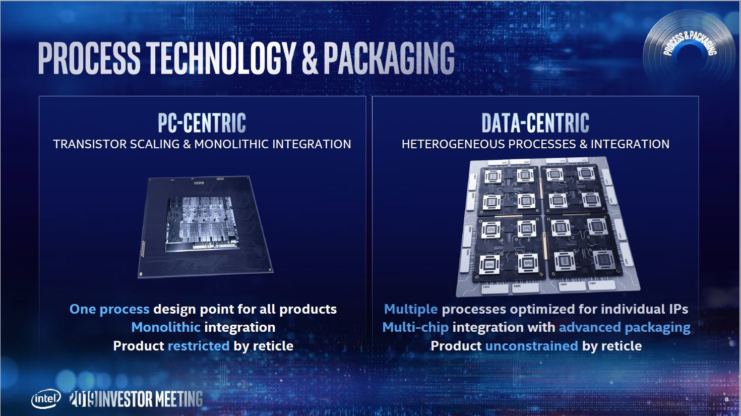
Apple to Launch Arm-Powered MacBook in the next 18 Months

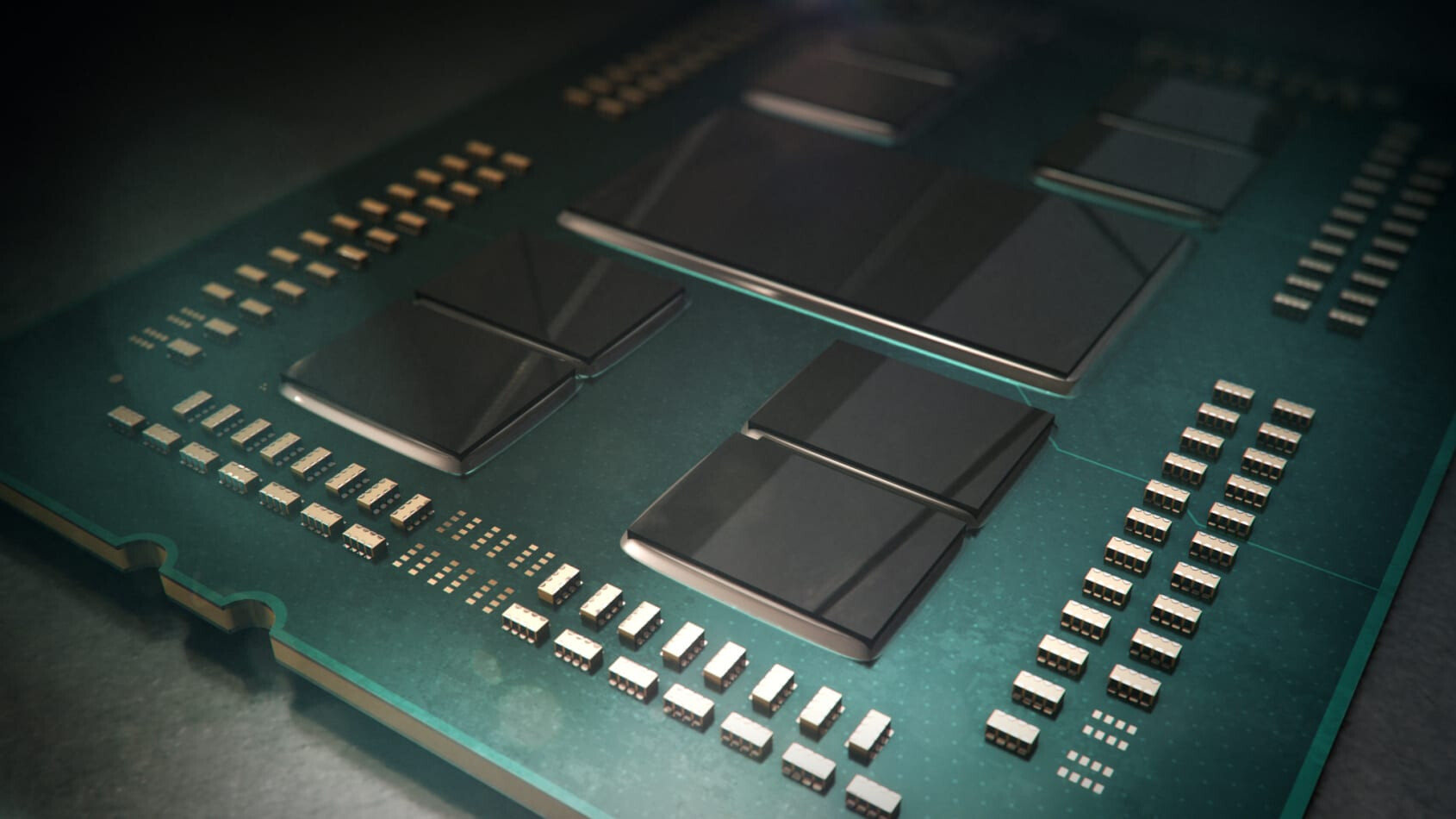
Apple is currently designing a custom series of CPUs, for its Macbook laptop lineup, based on the Arm Instruction Set Architecture. Having designed some of the most powerful mobile processors that are inside the iPhone series of devices, Apple is preparing to make a jump to an even more powerful device lineup by bringing custom CPUs for MacBook. Tired of the speed by which Intel replaces and upgrades its Core lineup of CPUs, Apple decided to take the matter in its own hands and rumors about the switch to a custom solution have been going on for a while. However, we now have some information about when to expect the first wave of Arm-powered Macs.

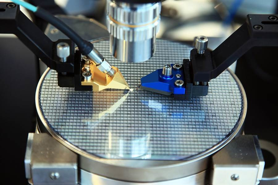
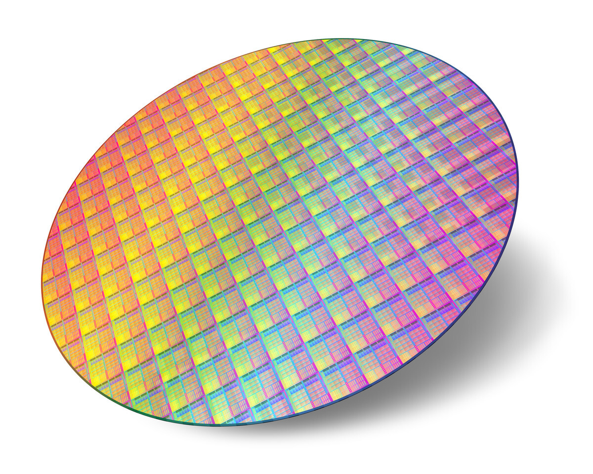
According to the analyst Ming-Chi Kuo, who is a well-known insider in the Apple industry, we can expect the first wave of the Arm-powered Macbook in the next 18 months, precisely in the first half of 2021. Supposedly, the first chips for these new Macs are going to be manufactured on a 5 nm manufacturing process, possibly over at TSMC since Apple had a long-lasting history of manufacturing its chips at TSMC foundries. In the meantime, we can expect to see Apple providing developers with tools to transition their x86-64 software to the new Arm ISA. Without a software ecosystem, the hardware platform is essentially worthless. And Apple knows this. We will see how they plan to play it and will report as soon as there is more information.

AMD to Outpace Apple as TSMC's Biggest 7nm Customer in 2020

AMD in the second half of 2020 could outpace Apple as the biggest foundry customer of TSMC for its 7 nm silicon fabrication nodes (DUV and EUV combined). There are two key factors contributing to this: AMD significantly increasing its orders for the year; and Apple transitioning to TSMC's 5 nm node for its A14 SoC, freeing up some 7 nm allocation, which AMD grabbed. AMD is currently tapping into 7 nm DUV for its "Zen 2" chiplet, "Navi 10," and "Navi 14" GPU dies. The company could continue to order 7 nm DUV until these products reach EOL; while also introducing the new "Renoir" APU die on the process. The foundry's new 7 nm+ (EUV) node will be utilized for "Zen 3" chiplets and "Navi 2#" GPU dies in 2020.

Currently, the top-5 customers for TSMC 7 nm are Apple, HiSilicon, Qualcomm, AMD, and MediaTek. Barring AMD, the others in the top-5 build mobile SoCs or 4G/5G modem chips on the node. AMD is expected to top the list as it scales up orders with TSMC. In the first half of 2020, TSMC's monthly output for 7 nm is expected to grow to 110,000 wafers per month (wpm). Apple's migration to 5 nm in 2H-2020, coupled with capacity-addition could take TSMC's 7 nm output to 140,000 wpm. AMD has reportedly booked the entire capacity-addition for 30,000 wpm, taking its allocation up to 21% in 2H-2020. Qualcomm is switching to Samsung for its next-generation SoCs and modems designed for 7 nm EUV. NVIDIA, too, is expected to built its next-gen 7 nm EUV GPUs on Samsung instead of TSMC. These moves by big players could free up significant foundry allocation at TSMC for AMD's volumes to grow in 2020.

AMD "Zen 4" 2021 Launch On Track as TSMC Optimistic About 5 nm

AMD's "Zen 4" CPU microarchitecture is on track for a 2021 launch as its principal foundry partner, TSMC, is optimistic about early yields of its 5 nm silicon fabrication node. TSMC supports the 5 nm product roadmaps of not just AMD, but also Apple and HiSilicon. "Zen 4" is particularly important for AMD, as it will release its next enterprise platform, codenamed "Genoa," along with the new SP5 socket. The new socket will present AMD with the opportunity to significantly change the processor's I/O, such as support for a new memory standard, a new PCIe generation, more memory channels, more PCIe lanes, etc. As early as 2019, the foundry is seeing yields of over 50 percent for the 5 nm node (possibly risk production designed to test the node), which is very encouraging for its customers.

AMD's roadmap for 2020 sees the introduction of "Zen 3" on the 7 nm EUV process (dubbed 7 nm+). AMD recently commented that the performance uplift of "Zen 3" versus "Zen 2" will be "right in line with what you would expect from an entirely new architecture." The 7 nm EUV node provides a significant 20 percent increase in transistor-density compared to the current 7 nm DUV node "Zen 2" chiplets and the company's "Navi" family of GPUs are built on. "Zen 3" could see the company do away with the CCX (quad-core CPU complex), and make chiplets monolithic blocks of CPU cores without sub-divisions. For the client-segment, 5 is a recurring number in 2021. It will see the introduction of the 5th generation Ryzen processors (5000-series), built on the 5 nm process, supporting DDR5 memory, PCI-Express gen 5, and the new AM5 client-segment CPU socket.

TSMC on Track to Deliver 3 nm in 2022

TSMC is delivering record results day after day, with a 5 nm manufacturing process starting High Volume Manufacturing (HVM) in Q2 next year, 7 nm process getting plenty of orders and the fact that TSMC just became the biggest company publicly trading in Asia. Continuing with the goal to match or even beat the famous Moore's Law, TSMC is already planning for future 3 nm node manufacturing, promised to start HVM as soon as 2022 arrives, according to JK Wang, TSMC's senior vice president of fab operations. Delivering 3 nm a whole year before originally planned in 2023, TSMC is working hard, with fab construction work doing quite well, judging by all the news that the company is releasing recently.

We can hope to see the first wave of products built using 3 nm manufacturing process sometime around end of year 2022, when the holiday season arrives. Usual customers like Apple and HiSilicon will surely utilize the new node and deliver their smartphones with 3 nm processors inside as soon as the process is ready for HVM.

TSMC: 5 nm on Track for Q2 2020 HVM, Ramping Faster than 7 nm

TSMC vice chairman and CEO C.C. Wei announced the company's plans for 5 nm are on track, which means High Volume manufacturing (HVM) on the node is expected to be achieved by 2Q 2020. The company has increased expenditures in ramping up its various nodes from an initially projected $10 billion to something along the lines of $14 billion - 15 billion; the company is really banking on quick uptake and design wins on its most modern process technologies - and the increased demand that follows.

TSMC's 5 nm process (N5) will use extreme ultraviolet lithography (EUVL) in many more layers than its N7+ and N6 processes, with up to 14 layers being etched in the N5 silicon compared to five and six, respectively, for its "older" N7+ and N6 processes. As the company increases capital expenditure in acquiring EUVL-capable equipment that sets up its production nodes for the market they foresee will just gobble up the chips in 2020, the company is optimistic they can achieve growth in the 5-10% number.

Moore's Law - Is it Really Dead ?

"Moore's Law" is a term coined in 1965 by Gordon Moore, who presented a paper which predicts that semiconductor scaling will allow integrated circuits to feature twice as many transistors present per same area as opposed to a chip manufactured two years ago. That means we could get same performance at half the power than the previous chip, or double the performance at same power/price in only two years time. Today we'll investigate if Moore's Law stayed true to its cause over the years and how much longer can it keep going.

TSMC to Begin Mass Production of 5nm Chips in 2020

According to industry sources over at DigiTimes, TSMC will begin mass production of its 5 nm node in March 2020, when companies using the 5 nm PDK can tape out their designs and integrate them into future products. Going into volume production two years after the 7 nm node, 5 nm is trying to put Moore's Law back on track again.

Built using the Extreme Ultra-Violet lithography (also known as EUV), 5 nm node is supposed to utilize existing FinFET transistors along with many improvements in speed, power and density when compared to existing 7 nm node. Speed is supposed to increase by around 15%, while density will improve by as much as 80%, which is excellent news for everyone. Noticeable power reduction is also present and it is now possible to have about 30% reduction in power consumption, while also enjoying additional speed and density improvements that new node brings.

Intel Switches Gears to 7nm Post 10nm, First Node Live in 2021

Intel's semiconductor manufacturing business has had a terrible past 5 years as it struggled to execute its 10 nanometer roadmap forcing the company's processor designers to re-hash the "Skylake" microarchitecture for 5 generations of Core processors, including the upcoming "Comet Lake." Its truly next-generation microarchitecture, codenamed "Ice Lake," which features a new CPU core design called "Sunny Cove," comes out toward the end of 2019, with desktop rollouts expected 2020. It turns out that the 10 nm process it's designed for, will have a rather short reign at Intel's fabs. Speaking at an investor's summit on Wednesday, Intel put out its silicon fabrication roadmap that sees an accelerated roll-out of Intel's own 7 nm process.

When it goes live and fit for mass production some time in 2021, Intel's 7 nm process will be a staggering 3 years behind TSMC, which fired up its 7 nm node in 2018. AMD is already mass-producing CPUs and GPUs on this node. Unlike TSMC, Intel will implement EUV (extreme ultraviolet) lithography straightaway. TSMC began 7 nm with DUV (deep ultraviolet) in 2018, and its EUV node went live in March. Samsung's 7 nm EUV node went up last October. Intel's roadmap doesn't show a leap from its current 10 nm node to 7 nm EUV, though. Intel will refine the 10 nm node to squeeze out energy-efficiency, with a refreshed 10 nm+ node that goes live some time in 2020.

Intel Courting Samsung to Manufacture Xe GPUs?

Intel's Xe discrete GPU project head Raja Koduri recently visited a Samsung Electronics silicon fabrication facility in Korea at the backdrop of the company's major 5 nm EUV announcement. This sparks speculation that Koduri could be exploring Samsung's portfolio of sub-10 nm contract-manufacturing offerings to mass-produce Xe discrete GPUs. Intel's own foundry business is reeling with mounting pressure from the company's main breadwinner, the client and enterprise processor businesses, to get its 10 nm node on the road. Koduri's GPU would need to leverage higher transistor densities than what Intel's 10 nm could offer, given that rival AMD is already implementing 7 nm, and NVIDIA is expected to go sub-10 nm with its future generation of GPUs.

Samsung Successfully Completes 5nm EUV Development

Samsung Electronics Co., Ltd., a world leader in advanced semiconductor technology, today announced that its 5-nanometer (nm) FinFET process technology is complete in its development and is now ready for customers' samples. By adding another cutting-edge node to its extreme ultraviolet (EUV)-based process offerings, Samsung is proving once again its leadership in the advanced foundry market.

Compared to 7 nm, Samsung's 5 nm FinFET process technology provides up to a 25 percent increase in logic area efficiency with 20 percent lower power consumption or 10 percent higher performance as a result of process improvement to enable us to have more innovative standard cell architecture. In addition to power performance area (PPA) improvements from 7 nm to 5 nm, customers can fully leverage Samsung's highly sophisticated EUV technology. Like its predecessor, 5 nm uses EUV lithography in metal layer patterning and reduces mask layers while providing better fidelity.

TSMC Completes 5 nm Design Infrastructure, Paving the Way for Silicon Advancement

TSMC announced they've completed the infrastructure design for the 5 nm process, which is the next step in silicon evolution when it comes to density and performance. TSMC's 5 nm process will leverage the company's second implementation of EUV (Extreme Ultra Violet) technology (after it's integrated in their 7 nm process first), allowing for improved yields and performance benefits.

According to TSMC, the 5 nm process will enable up to 1.8x the logic density of their 7 nm process, a 15% clock speed gain due to process improvements alone on an example Arm Cortex-A72 core, as well as SRAM and analog circuit area reduction, which means higher number of chips per wafer. The process is being geared for mobile, internet, and high performance computing applications. TSMC also provides online tools for silicon design flow scenarios that are optimized for their 5 nm process. Risk production is already ongoing.

AMD Says Not to Count on Exotic Materials for CPUs in the Next Ten Years, Silicon Is Still Computing's Best Friend

AMD's senior VP of AMD's datacentre group Forrest Norrod, at the Rice Oil and Gas HPC conference, said that while graphene does have incredible promise for the world of computing, it likely will take some ten years before such exotic material are actually taken advantage off. As Norrod puts it, silicon still has a pretty straightforward - if increasingly complex - path down to 3 nanometer densities. And according to him, at the rate manufacturers are being able to scale down their production nodes further, the average time between node transitions stands at some four or five years - which makes the jump to 5 nm and then 3 nm look exactly some 10 years from now, where Norrod expects to go through two additional shrinking nodes for the manufacturing process.

Of course, graphene is being hailed as the next best candidate for taking over silicon's place at the heart of our more complex, high-performance electronics, due, in part, to its high conductivity independent of temperature variation and its incredible switching resistance - it has been found to be able to operate at Terahertz switching speeds. It's a 2D material, which means that implementations of it will have to occur in deposited sheets of graphene across some other material.

GlobalFoundries Looking for Buyers, Samsung and SK Hynix Seem Interested

GlobalFoundries is looking to be sold lock-stock-and-barrel by its investors, after heavily downsizing and parting with some of its Singapore-based assets recently. Once promising to lead the market with 7 nm and 5 nm advancements, the company crashed out of the sub-10 nm race, making AMD, its biggest customer, look for 7 nm supplies from TSMC. GlobalFoundries is the world's third largest semiconductor foundry service provider, with an 8.4 percent market share, behind TSMC and Samsung. Intel doesn't offer manufacturing services, as its fabs are fully dedicated to manufacturing its own products.

GlobalFoundries's main investor is Abu Dhabi-based Mubadala Technology, which holds a 90 percent stake in the company. Korean semiconductor companies Samsung and SK Hynix are reportedly in the foray to buy out GlobalFoundries, as it would give them a turnkey presence in the US, with its Upstate New York facilities. The company is unlikely to entertain bids from Chinese companies, as CFIUS would likely block the sale. "Global Foundries is unlikely to be bought by a Chinese company such as SMIC in that the U.S. government is keeping China in check in various industries," said an industry insider, adding, "The most potential candidates include South Korean companies such as Samsung Electronics and SK Hynix, and Samsung Electronics can increase its share in the market to 23 percent at once if it takes over Global Foundries."

TSMC 7nm EUV Process to Enter Mass-Production in March 2019

TSMC is giving final touches to set its flagship 7 nanometer EUV (extreme ultraviolet lithography) silicon fabrication node at its highest state of readiness for business, called mass-production. At this state, the node can mass-produce products for TSMC's customers. TSMC had taped out its first 7 nm EUV chips in October 2018. The company will also begin risk-production of the more advanced 5 nm node in April, staying on schedule. Mass production of 5 nm chips could commence in the first half of 2020.

The 7 nm EUV node augments TSMC's 7 nm DUV (deep ultraviolet lithography) node that's been already active since April 2018, and producing chips for AMD, Apple, HiSilicon, and Xilinx. At the turn of the year, 7 nm DUV made up 9 percent of TSMC's shipments. With the new node going online, 7 nm (DUV + EUV) could make up 25 percent of TSMC's output by the end of 2019.

TSMC Cleared to Build New 3 nm Manufacturing Factory in Southern Taiwan

The world's largest contract semiconductor manufacturing company, TSMC, has been cleared to commence construction of a new 3 nm chip factory at the Southern Taiwan Science Park in Tainan. The new factory is expected to use 20 percent renewable energy and 50 percent recycled water.

The factory's environmental impact assessment was accepted by the Environmental Protection Administration (EPA) on Dec. 19, after concerns were raised about use of water and power sources. TSMC is expected to invest NT$600 million (US$19.45 million) in the project, with construction to begin in 2022. Production is planned to start in late 2022 or early 2023. At the same site, TSMC is also building a 5 nm chip factory, which is expected to be up and running in late 2019 or early 2020.

TSMC Increases Industry Foothold With 11.6% Increase in Revenue for Q3 2018

TSMC has quickly (over a span of years, but still) become the de-facto silicon manufacturing giant in the industry. They produce silicon-based solutions for almost all the significant tech companies (NVIDIA, AMD, Apple, Qualcomm, including the silicon manufacturing leader of yonder, Intel), and are on the forefront of new fabrication technologies. Just today we've covered how they are already well on their way to their second-gen 7 nm (N7+) fabrication technology with usage of EUV, and carving their path forward for 5 nm (N5).

TSMC 7 nm Second-Generation EUV Chips Taped Out, 5 nm Risk Production in April 2019

TSMC, the world's biggest contract semiconductor manufacturer, who is at the forefront of 7 nanometer production has just announced that they are making good progress with their second generation of 7 nm technology "N7+", using EUV (Extreme Ultraviolet Lithography). A first design for N7+ from an unnamed customer has been taped out. The company's first-gen 7 nm production is running well already, with final products, like Apple iPhone already in the hands of customers.

While not fully EUV yet, the N7+ process will see limited EUV usage, for up to four non-critical layers, which gives the company an opportunity to figure out how to make best use of the new technology, how to ramp up for mass production and how to fix the little quirks that show up as soon as you move from the lab to the factory.

Intel At Least 5 Years Behind TSMC and May Never Catch Up: Analyst

Intel's in-house sub-10 nanometer silicon fabrication dreams seem more distant by the day. Raymond James analyst Chris Caso, in an interview with CNBC stated that Intel's 10 nm process development could set the company back by at least 5 years behind TSMC. In its most recent financial results call, Intel revised its 10 nm outlook to reflect that the first 10 nm processors could only come out by the end of 2019. "Intel's biggest strategic problem is their delay on 10nm production - we don't expect a 10nm server chip from Intel for two years," analyst Chris Caso said in a note to clients Tuesday. "10nm delays create a window for competitors, and the window may never again close."

By that time, Intel will have missed several competitive milestones behind TSMC, which is in final stages of quantitatively rolling out its 7 nm process. Caso predicts that by the time Intel goes sub-10 nm (7 nm or something in that nanoscopic ballpark), TSMC and Samsung could each be readying their 5 nm or 3 nm process roll-outs. A Rosenblatt Securities report that came out late-August was even more gloomy about the situation at Intel foundry. It predicted that foundry delays could set the company back "5, 6, or even 7" years behind rivals. Intel is already beginning offload some of its 14 nm manufacturing to TSMC. Meanwhile, AMD is reportedly planning to entirely rely on TSMC to make its future generations of "Zen" processors.

TSMC to Bring 3D Stacked Wafers to Complex Silicon Designs, Such as GPUs

TSMC is close to adapt 3D stacked silicon wafers to complex silicon designs, such as graphics processors, using its new proprietary Wafer-on-Wafer (WoW) Advanced Packaging technology, which will be introduced with its 7 nm+ and 5 nm nodes. 3D stacked silicon fabrication is currently only implemented on "less complex" silicon designs, such as NAND flash, which don't run anywhere near as hot as complex designs ASIC designs, such as GPUs or CPUs. In its current form, TSMC achieved 2-layer stacks, in which two silicon layers that are "mirror images" of each other (for perfect alignment), sandwich bonding layers, through which pins for the upper layer pass through.

The bonding of the two layers is where the bulk of TSMC's innovations and "secret sauces" lie. For 3D NAND flash, multiple pancaked dies are wired out through their edges. You don't need as many pins to talk to a NAND flash die, as say a GPU die. For complex dies, designers have to pass thousands of pins through the "bottom layer," the connecting substrate, and eventually to the "top layer." The bottom layer hence is bumped out on both ends, one side interfacing with the package substrate for both dies, and the top side serving as a sort of substrate for the top die. This innovation is what TSMC calls "thru-silicon-vias" or TSVs.

Challenges With 7 nm, 5 nm EUV Technologies Could Lead to Delays In Process' TTM

Semiconductor manufacturers have been historically bullish when it comes to the introduction of new manufacturing technologies. Intel, AMD (and then Globalfoundries), TSMC, all are companies who thrive in investors' confidence: they want to paint the prettiest picture they can in terms of advancements and research leadership, because that's what attracts investment, and increased share value, and thus, increased funds to actually reach those optimistic goals.

However, we've seen in recent years how mighty Intel itself has fallen prey to unforeseen complications when it comes to advancements of its manufacturing processes, which saw us go from a "tick-tock" cadence of new architecture - new manufacturing process, to the introduction of 14 nm ++ processes. And as Intel, Globalfoundries and TSMC race towards sub 7-nm manufacturing processes with 250 mm wafers and EUV usage, things aren't getting as rosy as the ultraviolet moniker would make us believe.

TSMC to Build World's First 3 nm Fab in Taiwan

TSMC has announced the location for their first 3 nm fab: it will be built in the Tainan Science Park, southern Taiwan. Rumors pegged the new 3 nm factory as possibly being built in the US, due to political reasons; however, TSMC opted to keep their production capabilities clustered in the Tainan Science Park, where they can better leverage their assets and supply chain for the production and support of the world's first 3 nm semiconductor factory. It certainly also helped the Taiwanese government's decision to pledge land, water, electricity and environmental protection support to facilitate TSMC's latest manufacturing plan. It's expected that at least part of the manufacturing machines will be provided by ASML, a Netherlands-based company which has enjoyed 25% revenue growth already just this year.

As part of the announcement, TSMC hasn't given any revised timelines for their 3 nm production, which likely means the company still expects to start 3 nm production by 2022. TSMC said its 7 nm yield is ahead of schedule, and that it expects a fast ramp in 2018 - which is interesting, considering the company has announced plans to insert several extreme ultraviolet (EUV) layers at 7 nm. TSMC has also said its 5 nm roadmap is on track for a launch in the first quarter of 2019.

IBM Research Alliance Builds New Transistor for 5 nm Technology

IBM, its Research Alliance partners GLOBALFOUNDRIES and Samsung, and equipment suppliers have developed an industry-first process to build silicon nanosheet transistors that will enable 5 nanometer (nm) chips. The details of the process will be presented at the 2017 Symposia on VLSI Technology and Circuits conference in Kyoto, Japan. In less than two years since developing a 7 nm test node chip with 20 billion transistors, scientists have paved the way for 30 billion switches on a fingernail-sized chip.

The resulting increase in performance will help accelerate cognitive computing, the Internet of Things (IoT), and other data-intensive applications delivered in the cloud. The power savings could also mean that the batteries in smartphones and other mobile products could last two to three times longer than today's devices, before needing to be charged.

Samsung Announces Comprehensive Process Roadmap Down to 4 nm

Samsung stands as a technology giant in the industry, with tendrils stretching out towards almost every conceivable area of consumer, prosumer, and professional markets. It is also one of the companies which can actually bring up the fight to Intel when it comes to semiconductor manufacturing, with some analysts predicting the South Korean will dethrone Intel as the top chipmaker in Q2 of this year. Samsung scales from hyper-scale data centers to the internet-of-things, and is set to lead the industry with 8nm, 7nm, 6nm, 5nm, 4nm and 18nm FD-SOI in its newest process technology roadmap. The new Samsung roadmap shows how committed the company is (and the industry with it) towards enabling the highest performance possible from the depleting potential of the silicon medium. The 4 nm "post FinFET" structure process is set to be in risk production by 2020.

This announcement also marks Samsung's reiteration on the usage of EUV (Extreme Ultra Violet) tech towards wafer manufacturing, a technology that has long been hailed as the savior of denser processes, but has been ultimately pushed out of market adoption due to its complexity. Kelvin Low, senior director of foundry marketing at Samsung, said that the "magic number" for productivity (as in, with a sustainable investment/return ratio) with EUV is 1,500 wafers per day. Samsung has already exceeded 1,000 wafers per day and has a high degree of confidence that 1,500 wafers per day is achievable.

First 10 nm Intel Processor Out in 2017

With Intel's "tick-tock" product development cycle slowing down to a 3-launch cadence per silicon fab process, the company is preparing to launch no less than three micro-architectures on its next 10 nanometer silicon fab process. The first 10 nm CPU by Intel will launch in 2017.

In 2016, Intel will launch its 7th generation Core "Kaby Lake" processor, its third chip on the 14 nm process (after "Broadwell" and "Skylake"). The first 10 nm micro-architecture will be codenamed "Cannonlake," and will launch some time in 2017. Intel will build chips on the 10 nm for two more generations after "Cannonlake." The company's 2018 micro-architecture, built on the 10 nm will be codenamed "Icelake," and its 2019 release will be codenamed "Tigerlake." It's only 2020 that the company will pull out its next silicon fab process, 5 nm.

TSMC to Launch its 5 nm Fab by 2020

Taiwan's premier semiconductor foundry, TSMC, announced that it is on track to begin production of chips on its 7 nanometer silicon fab process by the first half of 2018. The company also announced that production on an even newer 5 nanometer process should commence two years later, in 2020. The company has currently cleared all decks for mass-production of chips on its 16 nm FFC (FinFET compact) node, with the company hoping to grab over 70% of the worldwide 14/16 nm production market-share by the end of 2016.
Return to Keyword Browsing
Apr 22nd, 2025 02:17 EDT change timezone

New Forum Posts

Popular Reviews

Controversial News Posts