Monday, October 21st 2024

Intel Arrow Lake-S Die Visibly Larger Than Raptor Lake-S, Die-size Estimated
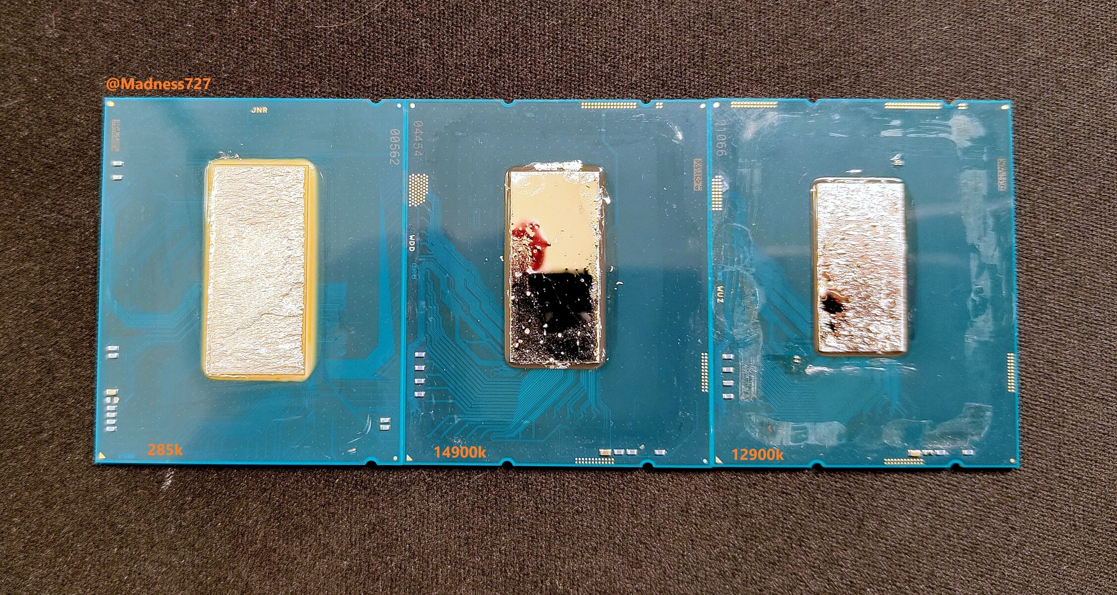
As a quick follow-up to last week's "Arrow Lake-S" de-lidding by Madness727, we now have a line-up of a de-lidded Core Ultra 9 285K "Arrow Lake-S" processor placed next to a Core i9-14900K "Raptor Lake-S," and the Core i9-12900K "Alder Lake-S." The tile-based "Arrow Lake-S" is visibly larger than the two, despite being made on more advanced foundry nodes. Both the 8P+16E "Raptor Lake-S" and 8P+8E "Alder Lake-S" chips are built on the Intel 7 node (10 nm Enhanced SuperFin). The "Raptor Lake-S" monolithic chip comes with a die-area of 257 mm². The "Alder Lake-S" is physically smaller, at 215 mm². What sets the two apart isn't just the two additional E-core clusters on "Raptor Lake-S," but also larger caches—2 MB of L2 per P-core, increased form 1.25 MB/core, and 4 MB per E-core cluster, increased from 2 MB/cluster.
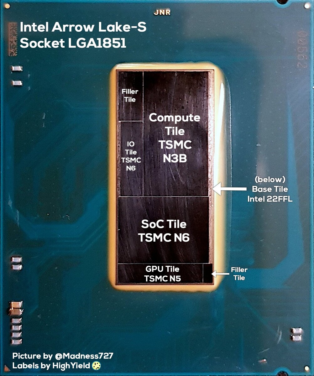
Thanks to high quality die-shots of the "Arrow Lake-S" by Madness727, we have our first die-area estimations by A Hollow Knight on Twitter. The LGA1851 fiberglass substrate has the same dimensions as the LGA1700 substrate. This is to ensure the socket retains cooler compatibility. Using geometrical measurements, the base tile of the "Arrow Lake-S" is estimated to be 300.9 mm² in area. The base-tile is a more suitable guideline for "die-area," since Intel uses filler tiles to ensure gaps in the arrangement of logic tiles are filled, and the chip aligns with the base-tile below. The base tile, built on an Intel 22 nm foundry node, serves like a silicon interposer, facilitating high-density microscopic wiring between the various logic tiles stacked on top, and an interface to the fiberglass substrate below.
 A Hollow Knight also put out his die-area estimations for each of the individual tiles. The Compute tile is estimated to measure 114.5 mm². This is the largest tile by area, and is built on the 3 nm TSMC N3B foundry node, and contains the CPU core complex with an 8P+16E core-count. The second-largest tile is the SoC tile, estimated to measure 86.1 mm². This tile is built on the 6 nm TSMC N6 node. The I/O tile is an extension of the SoC tile, it is built on the same 6 nm node, and is estimated to measure 23.79 mm².
The Graphics tile is, interestingly, smaller than even the I/O tile, and measures 22.8 mm². Intel built this on the 5 nm TSMC N5 node. It contains the brains of the iGPU, with 4 Xe cores, and other graphics rendering machinery. The media-accelerators, display controller, and display PHY components, are located on the SoC tile. Then there are the two filler tiles, the more visible of the two is the one next to the I/O tile, measuring 17 mm², and a smaller one next to the Graphics tile, measuring 2.6 mm². The filler tiles ensure the clump of logic tiles ends up having a rectangular form and a uniform Z-Height.
Interestingly, a slender, rectangular portion of the base tile remains exposed, with nothing stacked on top. This is what contributes to the 300.9 mm² die-area measurement by A Hollow Knight. If you were to simply add up the areas of the logic tiles, subtracting this exposed portion of the base tile, and the two filler tiles, you end up with 247.2 mm², which is in fact smaller than that of the monolithic "Raptor Lake-S."
Sources:
A Hollow Knight (Twitter), High Yield YT (Twitter), Madness727 (Twitter)
Thanks to high quality die-shots of the "Arrow Lake-S" by Madness727, we have our first die-area estimations by A Hollow Knight on Twitter. The LGA1851 fiberglass substrate has the same dimensions as the LGA1700 substrate. This is to ensure the socket retains cooler compatibility. Using geometrical measurements, the base tile of the "Arrow Lake-S" is estimated to be 300.9 mm² in area. The base-tile is a more suitable guideline for "die-area," since Intel uses filler tiles to ensure gaps in the arrangement of logic tiles are filled, and the chip aligns with the base-tile below. The base tile, built on an Intel 22 nm foundry node, serves like a silicon interposer, facilitating high-density microscopic wiring between the various logic tiles stacked on top, and an interface to the fiberglass substrate below.
The Graphics tile is, interestingly, smaller than even the I/O tile, and measures 22.8 mm². Intel built this on the 5 nm TSMC N5 node. It contains the brains of the iGPU, with 4 Xe cores, and other graphics rendering machinery. The media-accelerators, display controller, and display PHY components, are located on the SoC tile. Then there are the two filler tiles, the more visible of the two is the one next to the I/O tile, measuring 17 mm², and a smaller one next to the Graphics tile, measuring 2.6 mm². The filler tiles ensure the clump of logic tiles ends up having a rectangular form and a uniform Z-Height.
Interestingly, a slender, rectangular portion of the base tile remains exposed, with nothing stacked on top. This is what contributes to the 300.9 mm² die-area measurement by A Hollow Knight. If you were to simply add up the areas of the logic tiles, subtracting this exposed portion of the base tile, and the two filler tiles, you end up with 247.2 mm², which is in fact smaller than that of the monolithic "Raptor Lake-S."
13 Comments on Intel Arrow Lake-S Die Visibly Larger Than Raptor Lake-S, Die-size Estimated
And to consider Intel was joking at AMD one time for 'glue'... tsk tsk
So spreading out the cores is a good idea here...but I'm sure that can come with penalties in latency due to layout complexities. They'll have to continue weighing up whether they want to push the cores harder and get the heat out, or make things as compact as possible.
Side note, this is why I looked at the 11th gen before it launched and had a hunch it would overclock well from a thermal perspective (which was correct). It was going to be easier to get the heat out of the larger die-area:
This idea doesn't translate as easy with Arrow lake as it's on a new process and the tile layout complicates things further so we don't yet know (other than leaks/rumors) how much power the N3B node can handle. Rumors indicate it can't do much more clock speed on P-cores. Plenty of e-core headroom to get Cinebench improvements from, but that's not my favorite game lol. I'm curious how easy all the other "new features" are going to be to figure out for people who don't want to spend months fine-tuning their OC. We'll have to see the impact of die-to-die OC, memory OC, "dual BCLK tuning", etc.
Granted, "all" is a very strong word in the above sentence but ... that seven-lithic complexity is costly. It's not there to save a lot of money. N5 and N6 chiplets still cost a lot (price per transistor matters, not per mm²). Foveros bonding process can't be cheap, either. All in all, cost wise, it doesn't seem considerably cheaper than building a monolithic CPU. Or maybe, if N3 yields are still unacceptable, they could also choose to split the design in two chiplets, without the base tile. The AMD way basically but with a faster interconnect.
What has a cost for Arrow Lake is the 22nm interposer and packaging on top of that. On the other hand 22nm should be dirt cheap today and Intel definitely can manufacture 22nm very effectively. I bet running data over silicon has quite a sizeable efficiency advantage over running the same lines over substrate though.
Another thought ... the 22nm base die would actually be a suitable place for additional L3 cache, exactly because SRAM scaling is quite bad in the latest fab nodes. The SRAM cell size would be about 0.12 um² (Intel 22nm) against 0.02 um² (N3B). It's a simple structure compared to logic, requiring few metal layers. ~18 MB of cache would fit in a surface area 3x as large as the 36 MB of L3 on the compute die. That would leave enough space for all other signal and power wiring. Depending on how cheap 22nm is, and considering that L3 is not a big source of heat, it might even be economically justified.Yes. Low yields bring about two huge problems: high price and low availability. Here I'm just trying to guess which one is more huger for Intel at the moment.