AMD Instinct MI350X Series AI GPU Silicon Detailed
AMD today unveiled its Instinct MI350X series AI GPU. Based on the company's latest CDNA 4 compute architecture, the MI350X is designed to compete with NVIDIA B200 "Blackwell" AI GPU series, with the top-spec Instinct MI355X being compared by AMD to the B200 in its presentation. The chip debuts not just the CDNA 4 architecture, but also the latest ROCm 7 software stack, and hardware ecosystem based on the industry-standard Open Compute Project specification, which combines AMD EPYC Zen 5 CPUs, Instinct MI350 series GPUs, AMD-Pensando Pollara scale-out NICs supporting Ultra-Ethernet, and industry-standard racks and nodes, both in air- and liquid-cooled form-factors.
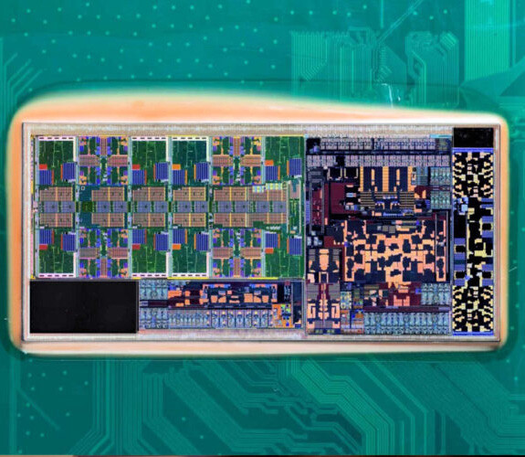
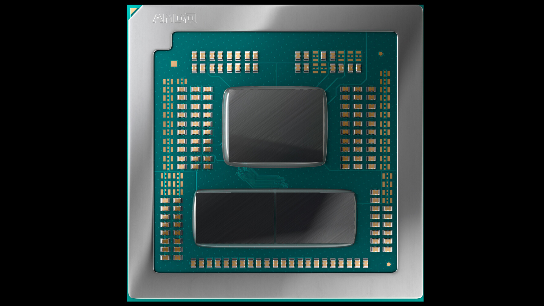
The MI350 is a gigantic chiplet-based AI GPU that consists of stacked silicon. There are two base tiles called I/O dies (IODs), each built on the 6 nm TSMC N6 process. This tile has microscopic wiring for up to four Accelerator Compute Die (XCD) tiles stacked on top, besides the 128-channel HBM3E memory controllers, 256 MB of Infinity Cache memory, the Infinity Fabric interfaces, and a PCI-Express 5.0 x16 root complex. The XCDs are built on the 3 nm TSMC N3P foundry node. These contain a 4 MB L2 cache, and four shader engines, each with 9 compute units. Each XCD hence has 36 CU, and each IOD seats 144 CU. Two IODs are joined at the hip by a 5.5 TB/s bidirectional interconnect that enables full cache coherency among the two IODs. The package has a total of 288 CU. Each IOD controls four HBM3E stacks for 144 GB of memory, the package has 288 GB.


The MI350 is a gigantic chiplet-based AI GPU that consists of stacked silicon. There are two base tiles called I/O dies (IODs), each built on the 6 nm TSMC N6 process. This tile has microscopic wiring for up to four Accelerator Compute Die (XCD) tiles stacked on top, besides the 128-channel HBM3E memory controllers, 256 MB of Infinity Cache memory, the Infinity Fabric interfaces, and a PCI-Express 5.0 x16 root complex. The XCDs are built on the 3 nm TSMC N3P foundry node. These contain a 4 MB L2 cache, and four shader engines, each with 9 compute units. Each XCD hence has 36 CU, and each IOD seats 144 CU. Two IODs are joined at the hip by a 5.5 TB/s bidirectional interconnect that enables full cache coherency among the two IODs. The package has a total of 288 CU. Each IOD controls four HBM3E stacks for 144 GB of memory, the package has 288 GB.