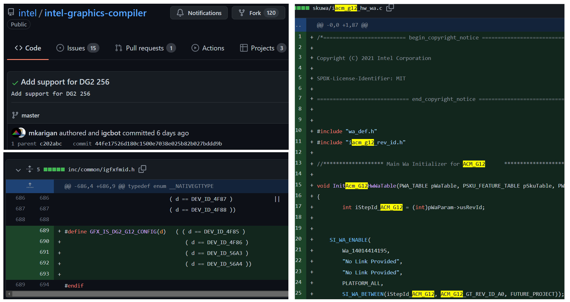
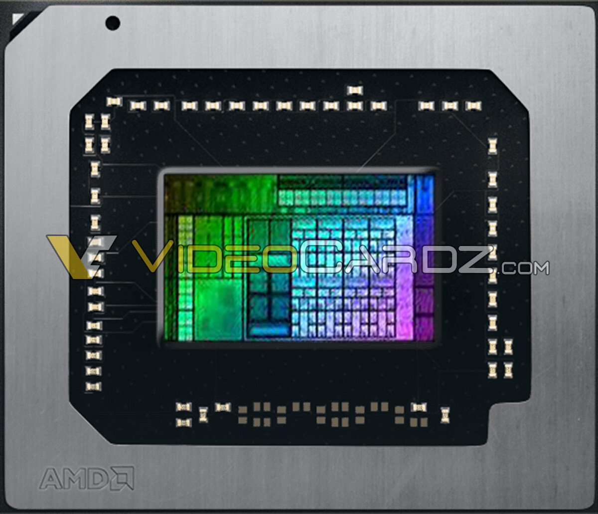
News Posts matching #6 nm

Return to Keyword Browsing

AMD Radeon "Navi 3x" Could See 50% Increase in Shaders, Double the Cache Memory

AMD's next generation Radeon "Navi 3x" line of GPUs could see a 50% increase in shaders and a doubling Infinity Cache memory size, according to some educated-guesswork and intelligence by Greymon55, a reliable source with GPU leaks. The Navi 31, Navi 32, and Navi 33 chips are expected to debut the new RDNA3 graphics architecture, and succeed the 6 nm optical-shrinks of existing Navi 2x chips that AMD is rumored to be working on.

The top Navi 31 part allegedly features 60 workgroup processors (WGPs), or 120 compute units. Assuming an RDNA3 CU still holds 64 stream processors, you're looking at 7,680 stream processors, a 50% increase over Navi 21. The Navi 32 silicon features 40 WGPs, and exactly the same number of shaders as the current Navi 21, at 5,120. The smallest of the three, the Navi 33, packs 16 WGPs, or 2,048 shaders. There is a generational doubling in cache memory, with 256 MB on the Navi 31, 192 MB on the Navi 32, and 64 MB on the Navi 33. Interestingly, the memory sizes and bus widths are unchanged, but AMD could leverage faster GDDR6 memory types. 2022 will see the likes of Samsung ship GDDR6 chips with data-rates as high as 24 Gbps.

NVIDIA Delays RTX 3070 Ti 16GB and RTX 3080 12GB Launches

NVIDIA has reportedly pushed midlife refreshes to its GeForce RTX 30-series "Ampere" graphics card family to beyond January, according to a report by Igor's Lab. The company was supposed to launch as many as three high-end graphics card SKUs in early-Q1, which include a 16 GB variant of the RTX 3070 Ti, which maxes out the GA104 silicon, a refreshed RTX 3080 12 GB variant, which keeps the CUDA core count of the original RTX 3080, but maxes out the 384-bit memory bus width of the GA102; and the RTX 3090 Ti, which maxes out both memory and CUDA cores on the GA102.

It's being reported that while the RTX 3090 Ti launch is on schedule, with announcements slated for NVIDIA's 2022 International CES presentation; the RTX 3070 Ti 16 GB and RTX 3080 12 GB could be launched only after the Chinese New Year (at least mid-February). The three SKUs, we predict, are designed to calibrate NVIDIA's lineup against a possible refresh of AMD's RDNA2 graphics architecture on the TSMC N6 (6 nm) node, which could allow the company to dial up engine clocks across the board, along with faster 18 Gbps GDDR6 memory, to better compete against the RTX 30-series. AMD is expected to announce these 6 nm GPUs in its CES presentation.

Qualcomm Expands Portfolio with Snapdragon 8cx Gen 3 and 7c+ Gen 3 To Accelerate Mobile Computing

During the annual Snapdragon Tech Summit, Qualcomm Technologies, Inc. expanded the portfolio of solutions for Always On, Always Connected PCs with the introduction of the Snapdragon 8cx Gen 3 compute platform, designed to deliver the performance and exceptional experiences users deserve in premium ultra-slim and fanless laptops. To strengthen the entry-tier Windows PC and Chromebook ecosystems with robust 5G connectivity and advanced AI experiences, the Company also unveiled the Snapdragon 7c+ Gen 3 Compute Platform. Both platforms utilize smart, connected technology to modernize PC experiences and redefine mobile computing for end users.

"Snapdragon 8cx Gen 3 builds on the technology that has transformed the PC industry, delivering premium experiences with breakthrough performance per watt, immersive camera and audio with enhanced AI-acceleration, lightning-fast 5G connectivity, and chip-to-cloud security in thin, fanless systems," says Miguel Nunes, vice president, product management, Qualcomm Technologies, Inc. "With Snapdragon 7c+ Gen 3, we are raising the bar in the entry-tier by extending 5G mobile computing across ecosystems. Whether for consumers, business, or education, Snapdragon compute platforms deliver the capabilities and experiences that our ecosystem customers and end users need."

ASUS Prepares ROG Zephyrus Duo GX650 Laptop With Upcoming AMD Ryzen 9 6900HX and NVIDIA GeForce RTX 3080 Ti

Prominent chip designers like AMD and NVIDIA could bless consumers with a broader offering of their new products as soon as CES 2022 arrives. AMD should present its rumored Rembrandt-H lineup of processors based on the enhanced Zen 3 core, sometimes referred to as Zen 3+. According to the latest report coming from MyLaptopsGuide, Bluetooth SIG has some data entry about ASUS'es upcoming ROG Zephyrus Duo GX650 laptop that integrates AMD Rembrandt-H processors and NVIDIA GeForce RTX 30-series graphics. As the website claims, the heart of this laptop will be AMD Ryzen 9 6900HX processor built on TSMC's 6 nm manufacturing process. We don't know much about this model, but we expect it to refine the previous Ryzen 9 5900HX.

We again see the rumored NVIDIA GeForce RTX 3080 Ti graphics card for mobile, powering the graphics side of things. This model is supposedly based on GA103S GPU SKU, which is likely tailor-made for laptops in mind and exclusive to them. ASUS has also paired 16 GB of DDR5-4800 RAM with an AMD Ryzen processor, suggesting that Rembrandt-H has a new memory controller in place. This laptop model also has a 16-inch 300 Hz Full HD screen with anti-glare; however, the amount of information ended there. We have to wait for CES 2022 launch to find out more.

AMD Posts November Investor Presentation

AMD later this month is preparing to address investors as part of a yet-unknown event. The company typically hosts Financial Analyst Day events around Q1-Q2, and goes to the investors with substantial material on the current state of the organization, the products on offer, what's on the horizon, and how it could impact the company's financials. An alleged presentation related to the November 2021 event was leaked to the web. The presentation provides a guided tour of the entire product portfolio of the company, spanning server processors, compute accelerators, consumer graphics, some client processors, and the semi-custom business.

The presentation outlines that the company has so far successfully executed its roadmaps for the client-CPU, server-CPU, graphics, and compute-accelerator segments. In the client CPU segment, it shows a successful execution up to 2021 with the "Zen 3" microarchitecture. In the server space, it mentions successful execution for its EPYC processors up to "Zen 3" with its "Milan" processors, and confirms that its next-generation "Zen 4" microarchitecture, and its sister-architecture, the "Zen 4c," will be built on the 5 nm silicon fabrication node (likely TSMC N5). The presentation also details the recently announced "Milan-X" processor for existing SP3 platforms, which debuts the 3D Vertical Cache technology, bringing up to 96 MB of L3 cache per CCD, and up to 768 MB of L3 cache (804 MB L1+L2+L3 cache) per socket.
Update 10:54 UTC: The presentation can now be found on the AMD Investor Relations website.

TSMC 3 nm To Enter Volume Production in 2022

TSMC will commercialize its N3 (3 nm) EUV silicon fabrication node in 2022, with volume production set to commence in the second half of the year. The company is looking to maximize capacity on its current N5 (5 nm) node, which already serves major customers such as Apple. AMD is expected to utilize N5 allocation going into 2022 as its next-generation "Zen 4" processors are expected to leverage the node to drive up CPU core counts and caches. The company is also utilizing N6 (6 nm) for its CDNA2 compute accelerator logic dies. N5 could also power mobile application processors from several manufacturers.

AMD Instinct MI200: Dual-GPU Chiplet; CDNA2 Architecture; 128 GB HBM2E

AMD today announced the debut of its 6 nm CDNA2 (Compute-DNA) architecture in the form of the MI200 family. The new, dual-GPU chiplet accelerator aims to lead AMD into a new era of High Performance Computing (HPC) applications, the high margin territory it needs to compete in for continued, sustainable growth. To that end, AMD has further improved on a matured, compute-oriented architecture born with Graphics Core Next (GCN) - and managed to improve performance while reducing total die size compared to its MI100 family.

Qualcomm Announces Updated Snapdragon 7, 6 and 4 Series Processors

Qualcomm Technologies, Inc. introduced four new mobile platforms - Snapdragon 778G Plus 5G, 695 5G, 480 Plus 5G, and 680 4G - to enable increased performance and capabilities across our high-, mid-, and entry-tiers. These 5G and 4G mobile platforms enable increased performance and capabilities to provide OEMs with additional options to help meet the existing demand.

There is significant traction and momentum across all Snapdragon tiers. By bringing cutting-edge features from the Snapdragon 8-series into the 7-, 6-, and 4-series, it is contributing to the growing demand across each Snapdragon series. The Snapdragon 7-series has grown by 44% in the last year alone due to tremendous high-tier demand. In the 6-series, consumer trends are emerging that show mid-tier smartphones will be the main driver for 5G adoption especially in emerging regions. Additionally, after less than one year, there have been more than 85 devices announced or in development based on the Snapdragon 480.

TSMC Rumoured to Build New Fab in Southern Taiwan

According to Nikkei, TSMC is set to start building a new fab in Kaohsiung, which is Taiwan's third largest city and located in the south of the island. It's also where ASE Technology Holding is located, which is the world's largest chip packaging and testing contractor. So far, TSMC doesn't have any fabs this far south in Taiwan, but it's not without its challenges.

The new fab is said to be designed to build chips on TSMC's 6 and 7 nm nodes, which are currently their most popular nodes, although this is likely to change as their 5 nm node begins to ramp up production. That said, there will still continue to be a huge demand for 6 and 7 nm parts, as these nodes transition to become mainstream production nodes.

Xbox Series S Refresh Rumored to Feature 6 nm AMD APU with 20+ Compute Units

Microsoft is potentially looking to refresh the Xbox Series S in late 2022 with an upgraded 6 nm AMD APU according to Moore's Law is Dead. The upgraded processor would be manufactured on TSMC's 6N process which boasts higher yields and could allow Microsoft to enable all 24 Compute Units on the APU compared to the 20 they currently enable. This increase in Compute Units and a clock speed boost could potentially increase the console's performance by 50%. This updated model would come in at close to 350 USD representing a 50 USD premium however the existing model would be retained and see a price cut to 189-249 USD. The rumor also claims that Microsoft will refresh the Xbox Series X in 2023 or later.

Foundry Revenue for 2Q21 Reaches Historical High Once Again with 6% QoQ Growth Thanks to Increased ASP and Persistent Demand, Says TrendForce

The panic buying of chips persisted in 2Q21 owing to factors such as post-pandemic demand, industry-wide shift to 5G telecom technology, geopolitical tensions, and chronic chip shortages, according to TrendForce's latest investigations. Chip demand from ODMs/OEMs remained high, as they were unable to meet shipment targets for various end-products due to the shortage of foundry capacities. In addition, wafers inputted in 1Q21 underwent a price hike and were subsequently outputted in 2Q21. Foundry revenue for the quarter reached US$24.407 billion, representing a 6.2% QoQ increase and yet another record high for the eighth consecutive quarter since 3Q19.

Intel Xe HPG Graphics Architecture and Arc "Alchemist" GPU Detailed

It's happening, Intel is taking a very pointy stab at the AAA gaming graphics market, taking the fight to NVIDIA GeForce and AMD Radeon. The Arc "Alchemist" discrete GPU implements the Xe HPG (high performance gaming) graphics architecture, and offers full DirectX 12 Ultimate compatibility. It also offers contemporary features gamers want, such as XeSS, an AI-supersampling feature rivaling DLSS and FSR. There's a lot more to the Xe HPG architecture than being a simple a scale-up from the Xe LP-based iGPUs found in today's "Tiger Lake" processors.

Just like Compute Units on AMD GPUs, and Streaming Multiprocessors on NVIDIA, Intel designed a scalable hierarchical compute hardware structure for Xe HPG. It begins with the Xe-core, an indivisible compute building block that contains 16 each of 256-bit vector engines and 1024-bit matrix engines. combined with basic load/store hardware and an L1 cache. The vector unit here is interchangeable with the execution unit, and the Xe-core contains 16 of these. The Render Slice is a collective of four Xe-cores, four Raytracing Units; and other common fixed-function hardware that include the geometry pipeline, rasterization pipeline, samplers, and pixel-backends. The Raytracing Units contain fixed-function hardware for bounding-box intersection, ray traversal, and triangle intersection.

Intel Beats AMD to 6nm GPUs, Arc "Alchemist" Built on TSMC N6 Process

In its 2021 Architecture Day presentation, Intel revealed that its first performance gaming GPU, the Arc "Alchemist," is built on the TSMC N6 silicon fabrication node (6 nm). A more advanced node than the N7 (7 nm) used by AMD for its current RDNA2 GPUs, TSMC N6 leverages EUV (extreme ultraviolet) lithography, and offers 18% higher transistor density, besides power improvements. "With N6, TSMC provides an optimal balance of performance, density, and power-efficiency that are ideal for modern GPUs," said Dr Kevin Zhang, SVP of Business Development at TSMC.

With working prototypes of "Alchemist" already internally circulating as the "DG2," Intel has beaten AMD to 6 nm. Team Red is reportedly planning optical-shrinks of its RDNA2-based "Navi 22" and "Navi 23" chips to TSMC N6, and assigning them mid-range SKUs in the Radeon RX 7000 series. The company will build two higher-segment RDNA3 GPUs on the more advanced TSMC N5 (5 nm) process, which will release in 2022, and power successors to the RX 6700 series and RX 6800/6900 series.

AMD Radeon RX 7000 Series to Include 6nm Optical-Shrinks of RDNA2

AMD's upcoming Radeon RX 7000 series could include GPUs from both the RDNA3 and RDNA2 graphics architectures, according to reliable sources on social media. This theory holds that the company could introduce new 5 nm GPUs based on the new RDNA3 architecture for the higher end, namely the Navi 31 and Navi 32; while giving the current-gen RDNA2 architecture a new lease of life in the lower segments. This isn't, however, a simple rebrand.

Apparently, some existing Navi 2x series chips will receive an optical shrink to the 6 nm node, in a bid to improve their performance/Watt. Some of the performance/Watt improvement could be used to increase engine clocks. These include the Navi 22, with its 40 RDNA2 compute units and 192-bit GDDR6 memory bus; and the Navi 23, with its 32 RDNA2 compute units and 128-bit GDDR6 memory bus. The updated Navi 22 will power the SKU that succeeds the current RX 6600 XT, while the updated Navi 23 works the lower-mainstream SKU RX x500-class.

Next-Gen AMD Radeon RDNA3 Flagship To Feature 15,360 Stream Processors?

AMD's next generation RDNA3 graphics architecture generation could see a near-quadrupling in raw SIMD muscle over the current RDNA2, according to a spectacular rumor. Apparently, the company will deploy as many as 15,360 stream processors (quadruple that of a Radeon RX 6800), and spread across 60 WGPs (Workgroup Processors), and do away with the compute unit. This is possibly because the RDNA3 compute unit won't be as independent as the ones on the original RDNA or even RDNA2, which begins to see groups of two CUs share common resources.

Another set of rumors suggest that AMD won't play NVIDIA's game of designing GPUs with wide memory bus widths, and instead build on its Infinity Cache technology, by increasing the on-die cache size and bandwidth, while retaining "affordable" discrete memory bus widths, such as 256-bit. As for the chip itself, it's rumored that the top RDNA3 part, the so-called "Navi 31," could feature a multi-chip module design (at least two logic dies), each with 30 WGPs. Each of the two is expected to be built on a next-gen silicon fabrication node that's either TSMC N5 (5 nm), or a special 6 nm node TSMC is designing for AMD. Much like the next-generation "Lovelace" architecture by NVIDIA, AMD's RDNA3 could see the light of the day only in 2022.

AMD Ryzen Embedded V3000 SoCs Based on 6nm Node, Zen 3 Microarchitecture

AMD's next generation Ryzen Embedded V3000 system-on-chips aren't simply "Cezanne" dies sitting on BGA packages, but rather based on a brand new silicon, according to Patrick Schur, a reliable source with leaks. The die will be built on the more advanced 6 nm silicon fabrication node, whilst still being based on the current "Zen 3" microarchitecture. There are several things that set it apart from the APU silicon of the current-generation, making it more relevant for the applications the Ryzen Embedded processor family is originally built for.

Built in the FP7r2 BGA package, the V3000 silicon features an 8-core/16-thread CPU based on the "Zen 3" microarchitecture. There are also an integrated GPU based on the RDNA2 graphics architecture, with up to 12 CUs, a dual-channel DDR5 memory interface, a 20-lane PCI-Express 4.0 root complex, with up to 8 lanes put out for PEG; two USB4 ports, and two 10 GbE PHYs. AMD could design at least three SKUs based on this silicon, spanning TDP bands of 15-30 W and 35-54 W.

Rumor: AMD Rembrandt APUs to Feature Zen3+, RDNA2 Architectures - Up to 12 CUs

A fresh rumor straight from the rumor mill paints AMD's next APU iterations as being updated to the latest and greatest architectures the company has to offer. The rumor comes from ExecutableFix via Twitter, a leaker who has a relatively proven track record on being right regarding upcoming hardware releases. This rumor can lay some credence to others, painting AMD's Ryzen 7000 series as being the first AMD APU-only release since they began their journey with the Zen architecture - it makes sense for the company to integrate their latest architectures in the mobile-geared Rembrandt first, working out some possible interaction quirks that might arise between the two architectures when deployed in the same package.

The leaker further affirms that the Rembrandt APUs will feature up to 12 RDNA2 CUs, which would amount to 768 stream processors on-chip - a marked increase from the current-generation 8 CUs based on the Vega architecture on their Ryzen 4000 mobile series. The leaker also discloses that AMD's Warhol seems to be MIA in recent AMD documentation and planning when it comes to the deployment of Zen3+, and that Rembrandt should be the one to carry that particular architecture refinement through to the 6 nm process. It would seem that AMD's Vega would "finally" see its demise, bringing about some much-needed performance improvements to counter Intel's investments in GPU performance with Xe.

Sony Reportedly Working on Redesigned PS5 SoC on 6 nm for 2022

It's not only graphics cards and CPUs that are best kept on the edge of manufacturing processes; in truth, one could even say that consoles have more to gain from these transitions when it comes to their manufacturers' financial outlooks. This happens because usually, consoles are subsidized by manufacturers in that their actual retail price is lower than manufacturing costs; this works as a way for console players to increase their platforms' attractiveness and user base, so they can then sell them games and subscription services, where the big bucks are actually made. We knew this already, but Microsoft's head of Xbox business development, Lori Wright confirmed it yesterday at the Apple vs Epic Games hearing. Lori Wright is quoted as answering "We don't; we sell the consoles at a loss" when asked whether Microsoft does or does not turn a profit on Xbox Series S | X hardware sales.

Considering the similarities between the Xbox Series X and PS5's SoC, it's very likely that Sony doesn't make a profit on console hardware sales either - or if it actually does, it's nothing actually meaningful. This is part of the reason why consoles are usually actually in the forefront of manufacturing processes' advancements, as it's a way for console players to quickly reduce the BoM (Bill of Materials) for their consoles. Since the specifications don't change within a console generation (discounting Pro models, which both companies have taken to launching some years into their generations), they choose to take advantage of process advancements due to the transistor density increases that allow for both lower silicon area for the SoC, and lower power consumption - which sometimes enables them to develop slim versions of their gaming consoles.

ASML Finishes Development of EUV Pellicles for Greater Sub-7nm Yields

ASML has finally finished development of EUV (Extreme Ultra Violet) pellicles to be employed in manufacturing processes that use the most energetic frequency of visible light to etch semiconductors onto wafers. Pellicles have been used for decades in the industry, and they are basically ultra-thin membranes that protect photomasks during the etching process - impeding particles from depositing in the substrate, which could lead to defects at the wafer level for every subsequent patterning that is laid on top of the impurity. Manufacturers such as TSMC have deployed EUV-powered manufacturing processes, but they have had to toil with potentially lower yields and increased costs with wafer analysis so as to reduce chances of defects appearing.

It's been a long time coming for EUV-capable pellicles, because these have different requirements compared to their traditional, non-EUV counterparts. However, once they are available on the market, it's expected that all semiconductor manufacturers with bleeding-edge manufacturing processes integrate them into their production flows. These will allow for better yields, which in turn should reduce overall pricing for the manufacturing processes. As an example, these EUV masks could be deployed on TSMC's 7 nm, 6 nm, 5 nm, and so on and so on. Other players other than ASML are also finishing their pellicle design, so the industry will have multiple options to integrate into their processes.

New Intel DG2 HPG GPU Surface, Could Power a Family of Products

It appears that Intel's DG2 refers to a number of HPG (High Performance Graphics) products within the same family, with rumors surfacing around a possible total of six different graphics products based on the company's latest high performance graphics architecture - and its debut on the high performance discrete market. It's been confirmed that Intel's DG2 products will not be manufactured in-house, via Intel's 10 nm SuperFin technology, but with recourse to foundry partner TSMC's 6 nm fabrication technology.

It seems that DG2 is currently slated for launch based on three different chip configurations: the first is the DG2 512EU, which will power the highest-performance, 4096 shading unit, 8 GB / 16 GB GDDR6 and 192-bit bus graphics card. Another chip is the DG12 384EU, estimated to come in at ~190 mm², available in three different shading unit configurations: 3072 shading units, with an accompanying 6/12 GB of GDDR6 memory and 192-bit bus; 2048 shading units, which reduces allotted memory to 4/8 GB configurations and a 128-bit memory bus; and finally, the further cut-down 1536 shading unit configuration, with a maximum of 4 GB of GDDR6 memory over the same 128-bit bus. The final (current) chip in the DG2 family is the DG2 128EU, with both 128EU and 96EU configurations (1024 and 768 shading units, respectively) carrying 4 GB VRAM over a pretty tight 64-bit bus. We'll see if these leaks actually materialize into final Intel products, and if these design choices are the possible best, considering Intel's technology, so as to assail the two-player party that is the discrete, high performance graphics market.

SiPearl to Manufacture its 72-Core Rhea HPC SoC at TSMC Facilities

SiPearl has this week announced their collaboration with Open-Silicon Research, the India-based entity of OpenFive, to produce the next-generation SoC designed for HPC purposes. SiPearl is a part of the European Processor Initiative (EPI) team and is responsible for designing the SoC itself that is supposed to be a base for the European exascale supercomputer. In the partnership with Open-Silicon Research, SiPearl expects to get a service that will integrate all the IP blocks and help with the tape out of the chip once it is done. There is a deadline set for the year 2023, however, both companies expect the chip to get shipped by Q4 of 2022.

When it comes to details of the SoC, it is called Rhea and it will be a 72-core Arm ISA based processor with Neoverse Zeus cores interconnected by a mesh. There are going to be 68 mesh network L3 cache slices in between all of the cores. All of that will be manufactured using TSMC's 6 nm extreme ultraviolet lithography (EUV) technology for silicon manufacturing. The Rhea SoC design will utilize 2.5D packaging with many IP blocks stitched together and HBM2E memory present on the die. It is unknown exactly what configuration of HBM2E is going to be present. The system will also see support for DDR5 memory and thus enable two-level system memory by combining HBM and DDR. We are excited to see how the final product looks like and now we wait for more updates on the project.

MediaTek Launches 6nm Dimensity 1200 Premium 5G SoC

MediaTek today unveiled its new Dimensity 1200 and Dimensity 1100 5G smartphone chipsets with unrivaled AI, camera and multimedia features for powerful 5G experiences. The addition of the 6 nm Dimensity 1200 and 1100 chipsets to MediaTek's 5G portfolio gives device makers a growing suite of options to design highly capable 5G smartphones with top of the line camera features, graphics, connectivity enhancements and more.

"MediaTek continues to expand its 5G portfolio with highly integrated solutions for a range of devices from the high-end to the mid-tier," said JC Hsu, Corporate Vice President and General Manager of MediaTek's Wireless Communications Business Unit. "Our new Dimensity 1200 stands out with its impressive 200MP camera support and advanced AI capabilities, in addition to its innovative connectivity, display, audio and gaming enhancements."

Intel Courts TSMC 6nm and 3nm Nodes for Future Xe GPU Generations

Intel is rumored to be aligning its future-generation Xe GPU development with TSMC's node development cycle, with the company reportedly negotiating with the Taiwanese foundry for 6 nm and 3 nm allocation for its large Xe GPUs. Intel's first Xe discrete GPUs for the market, however, are reportedly built on the company's own 10 nm+ silicon fabrication process.

While Intel's fascination with TSMC 3 nm is understandable, seeking out TSMC's 6 nm node raises eyebrows. Internally referred to as "N6," the 6 nm silicon fabrication node at TSMC is expected to go live either towards the end of 2020 or early 2021, which is when Intel's 10 nm+ node is expected to pick up volume production, beginning with the company's "Tiger Lake" processors. Perhaps a decision has been made internally to ensure that Xe doesn't eat too much into Intel's own foundry capacities meant for processor manufacturing, and to instead outsource Xe manufacturing to third-party foundries like TSMC and Samsung eventually. Way back in April 2019 it was rumored that Intel was evaluating Samsung as a foundry partner for Xe.

AMD RDNA2 Graphics Architecture Detailed, Offers +50% Perf-per-Watt over RDNA

With its 7 nm RDNA architecture that debuted in July 2019, AMD achieved a nearly 50% gain in performance/Watt over the previous "Vega" architecture. At its 2020 Financial Analyst Day event, AMD made a big disclosure: that its upcoming RDNA2 architecture will offer a similar 50% performance/Watt jump over RDNA. The new RDNA2 graphics architecture is expected to leverage 7 nm+ (7 nm EUV), which offers up to 18% transistor-density increase over 7 nm DUV, among other process-level improvements. AMD could tap into this to increase price-performance by serving up more compute units at existing price-points, running at higher clock speeds.

AMD has two key design goals with RDNA2 that helps it close the feature-set gap with NVIDIA: real-time ray-tracing, and variable-rate shading, both of which have been standardized by Microsoft under DirectX 12 DXR and VRS APIs. AMD announced that RDNA2 will feature dedicated ray-tracing hardware on die. On the software side, the hardware will leverage industry-standard DXR 1.1 API. The company is supplying RDNA2 to next-generation game console manufacturers such as Sony and Microsoft, so it's highly likely that AMD's approach to standardized ray-tracing will have more takers than NVIDIA's RTX ecosystem that tops up DXR feature-sets with its own RTX feature-set.
AMD GPU Architecture Roadmap RDNA2 RDNA3 AMD RDNA2 Efficiency Roadmap AMD RDNA2 Performance per Watt AMD RDNA2 Raytracing

UNISOC Launches Next-Gen 5G SoC T7520 on 6 nm EUV Manufacturing Node

UNISOC, a leading global supplier of mobile communication and IoT chipsets, today officially launched its new-generation 5G SoC mobile platform - T7520. Using cutting-edge process technology, T7520 enables an optimized 5G experience with substantially enhanced AI computing and multimedia imaging processing capabilities while lowering power consumption.

T7520 is UNISOC's second-generation 5G smartphone platform. Built on a 6 nm EUV process technology and empowered by some of the latest design techniques, it offers substantially enhanced performance at a lower level of power consumption than ever.
Return to Keyword Browsing
Aug 14th, 2024 13:43 EDT change timezone

New Forum Posts

Popular Reviews

Controversial News Posts