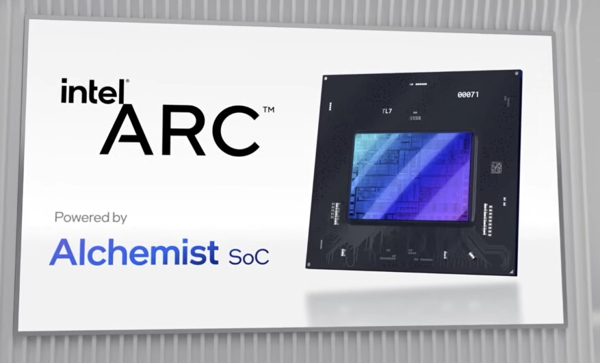
Intel Xe HPG Graphics Architecture and Arc "Alchemist" GPU Detailed
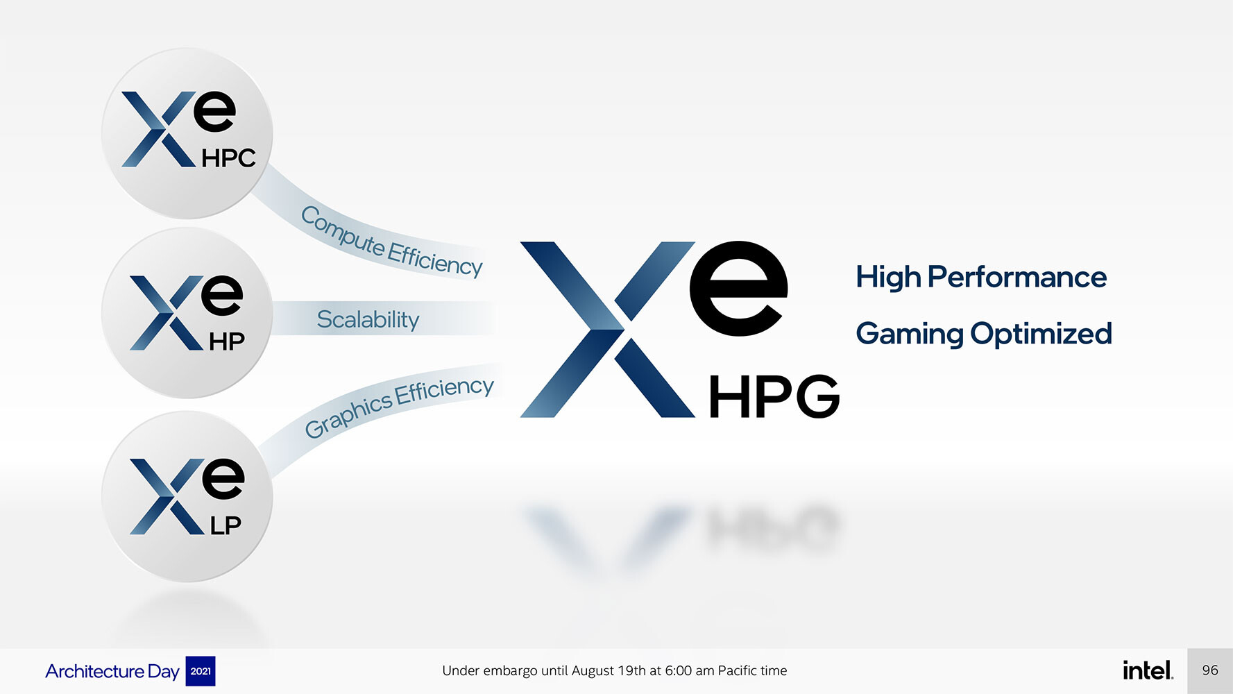
It's happening, Intel is taking a very pointy stab at the AAA gaming graphics market, taking the fight to NVIDIA GeForce and AMD Radeon. The Arc "Alchemist" discrete GPU implements the Xe HPG (high performance gaming) graphics architecture, and offers full DirectX 12 Ultimate compatibility. It also offers contemporary features gamers want, such as XeSS, an AI-supersampling feature rivaling DLSS and FSR. There's a lot more to the Xe HPG architecture than being a simple a scale-up from the Xe LP-based iGPUs found in today's "Tiger Lake" processors.
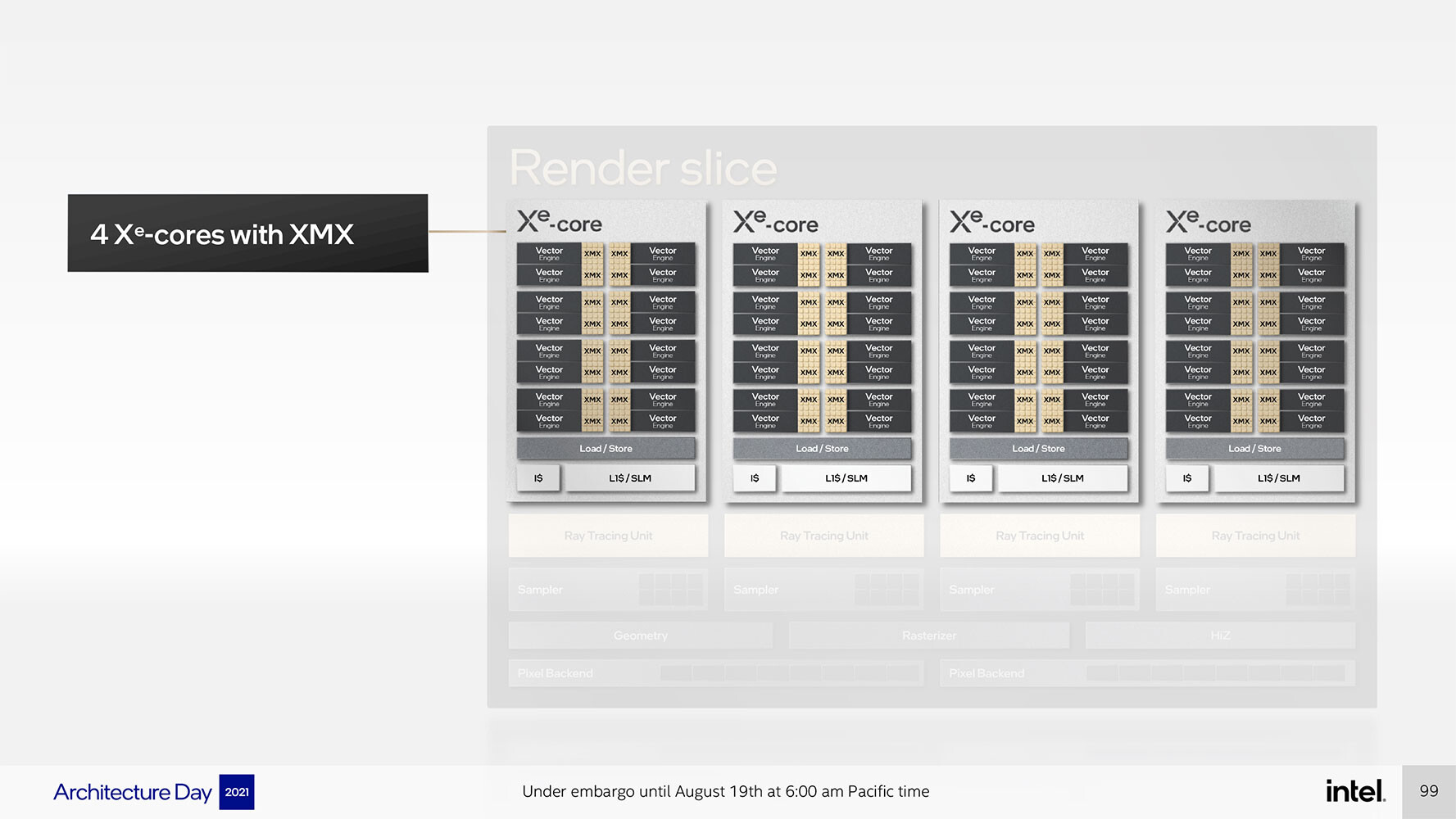
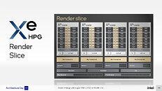
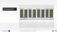
Just like Compute Units on AMD GPUs, and Streaming Multiprocessors on NVIDIA, Intel designed a scalable hierarchical compute hardware structure for Xe HPG. It begins with the Xe-core, an indivisible compute building block that contains 16 each of 256-bit vector engines and 1024-bit matrix engines. combined with basic load/store hardware and an L1 cache. The vector unit here is interchangeable with the execution unit, and the Xe-core contains 16 of these. The Render Slice is a collective of four Xe-cores, four Raytracing Units; and other common fixed-function hardware that include the geometry pipeline, rasterization pipeline, samplers, and pixel-backends. The Raytracing Units contain fixed-function hardware for bounding-box intersection, ray traversal, and triangle intersection.

Just like Compute Units on AMD GPUs, and Streaming Multiprocessors on NVIDIA, Intel designed a scalable hierarchical compute hardware structure for Xe HPG. It begins with the Xe-core, an indivisible compute building block that contains 16 each of 256-bit vector engines and 1024-bit matrix engines. combined with basic load/store hardware and an L1 cache. The vector unit here is interchangeable with the execution unit, and the Xe-core contains 16 of these. The Render Slice is a collective of four Xe-cores, four Raytracing Units; and other common fixed-function hardware that include the geometry pipeline, rasterization pipeline, samplers, and pixel-backends. The Raytracing Units contain fixed-function hardware for bounding-box intersection, ray traversal, and triangle intersection.