News Posts matching #LPDDR5

Return to Keyword Browsing

Nintendo Switch Successor: Backward Compatibility Confirmed for 2025 Launch

Nintendo has officially announced that its next-generation Switch console will feature backward compatibility, allowing players to use their existing game libraries on the new system. However, those eagerly awaiting the console's release may need to exercise patience as launch expectations have shifted to early 2025. On the official X account, Nintendo has announced: "At today's Corporate Management Policy Briefing, we announced that Nintendo Switch software will also be playable on the successor to Nintendo Switch. Nintendo Switch Online will be available on the successor to Nintendo Switch as well. Further information about the successor to Nintendo Switch, including its compatibility with Nintendo Switch, will be announced at a later date."

While the original Switch evolved from a 20 nm Tegra X1 to a more power-efficient 16 nm Tegra X1+ SoC (both featuring four Cortex-A57 and four Cortex-A53 cores with GM20B Maxwell GPUs), the Switch 2 is rumored to utilize a customized variant of NVIDIA's Jetson Orin SoC, now codenamed T239. The new chip represents a significant upgrade with its 12 Cortex-A78AE cores, LPDDR5 memory, and Ampere GPU architecture with 1,536 CUDA cores, promising enhanced battery efficiency and DLSS capabilities for the handheld gaming market. With the holiday 2024 release window now seemingly off the table, the new console is anticipated to debut in the first half of 2025, marking nearly eight years since the original Switch's launch.

JEDEC Publishes LPDDR5 CAMM2 Connector Performance Standard

JEDEC Solid State Technology Association, the global leader in standards development for the microelectronics industry, today announced the publication of PS-007A LPDDR5 CAMM2 Connector Performance Standard. The connector, referred to as "LP5CAMM2," is designed to offer a standardized modular LPDDR5 solution with ecosystem support, unlike the traditional LPDDR5 memory-down approach. Developed by JEDEC's JC-11 Committee for Mechanical Standardization, PS-007A is available for free download from the JEDEC website.

As compared to a DDR5 SODIMM connector, benefits of the LP5CAMM2 connector include:
  • Better signal integrity (SI) and improved radio frequency interference (RFI)
  • To enable a module solution with lower power consumption and increased battery life
  • 50% form factor reduction with the similar Z height

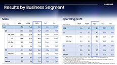
Samsung Electronics Announces Results for Third Quarter of 2024, 7 Percent Revenue Increase

Samsung Electronics today reported financial results for the third quarter ended Sept. 30, 2024. The Company posted KRW 79.1 trillion in consolidated revenue, an increase of 7% from the previous quarter, on the back of the launch effects of new smartphone models and increased sales of high-end memory products. Operating profit declined to KRW 9.18 trillion, largely due to one-off costs, including the provision of incentives in the Device Solutions (DS) Division. The strength of the Korean won against the U.S. dollar resulted in a negative impact on company-wide operating profit of about KRW 0.5 trillion compared to the previous quarter.

In the fourth quarter, while memory demand for mobile and PC may encounter softness, growth in AI will keep demand at robust levels. Against this backdrop, the Company will concentrate on driving sales of High Bandwidth Memory (HBM) and high-density products. The Foundry Business aims to increase order volumes by enhancing advanced process technologies. Samsung Display Corporation (SDC) expects the demand of flagship products from major customers to continue, while maintaining a quite conservative outlook on its performance. The Device eXperience (DX) Division will continue to focus on premium products, but sales are expected to decline slightly compared to the previous quarter.

Google's Upcoming Tensor G5 and G6 Specs Might Have Been Revealed Early

Details of what is claimed to be Google's upcoming Tensor G5 and G6 SoCs have popped up over on Notebookcheck.net and the site claims to have found the specs on a public platform, without going into any further details. Those that were betting on the Tensor G5—codenamed Laguna—delivering vastly improved performance over the Tensor G4, are likely to be disappointed, at least on the CPU side of things. As previous rumours have suggested, the chip is expected to be manufactured by TSMC, using its N3E process node, but the Tensor G5 will retain the single Arm Cortex-X4 core, although it will see a slight upgrade to five Cortex-A725 cores vs. the three Cortex-A720 cores of the Tensor G4. The G5 loses two Cortex-A520 cores in favour of the extra Cortex-A725 cores. The Cortex-X4 will also remain clocked at the same peak 3.1 GHz as that of the Tensor G4.

Interestingly it looks like Google will drop the Arm Mali GPU in favour of an Imagination Technologies DXT GPU, although the specs listed by Notebookcheck doesn't add up with any of the specs listed by Imagination Technologies. The G5 will continue to support 4x 16-bit LPDDR5 or LPDDR5X memory chips, but Google has added support for UFS 4.0 memory, something that's been a point of complaint for the Tensor G4. Other new additions is support for 10 Gbps USB 3.2 Gen 2 and PCI Express 4.0. Some improvements to the camera logic has also been made, with support for up to 200 Megapixel sensors or 108 Megapixels with zero shutter lag, but if Google will use such a camera or not is anyone's guess at this point in time.

AMD Ryzen Z2 Extreme to Feature a 3+5 Core Configuration

The second generation of AMD Ryzen Z-series processors for handheld gaming consoles, will be led by the Ryzen Z2 Extreme. There will also be an affordable Ryzen Z2 (non-Extreme). We've known for some time that the Z2 Extreme is based on the 4 nm "Strix Point" monolithic silicon, with some optimization (the highest bins to facilitate the best energy efficiency); but now we have a few more details thanks to a leak by Golden Pig Upgrade. AMD's engineering effort with the Z2 Extreme will be to give the console the most generational performance uplift from the iGPU, rather than the CPU.

The "Strix Point" silicon features a significantly updated iGPU from the previous-generation "Phoenix." It's based on the more efficient RDNA 3.5 graphics architecture, which is better optimized for LPDDR5 memory; and comes with 16 compute units (CU), compared to 12 on the "Phoenix." The Ryzen Z2 Extreme will come with all 16 CU enabled. The CPU is where some interesting changes are planned. The "Strix Point" silicon features a dual-CCX CPU, one of these contains four "Zen 5" CPU cores sharing a 16 MB L3 cache, while the other features eight "Zen 5c" cores sharing an 8 MB L3 cache. For the Ryzen Z2 Extreme, AMD is going with an odd 3+5 core configuration. What this means is that the Ryzen Z2 Extreme will have 3 "Zen 5" cores, and 5 "Zen 5c" cores. The L3 cache on the CCX with "Zen 5" cores has been reduced to 8 MB in size. On paper, this is still an 8-core/16-thread CPU with 16 MB of L3 cache (same as "Phoenix,") but now you know that there's more going on.

AAEON FWS-2290 Harnesses Intel Processor N97 for More Powerful Desktop Network Solutions

Leading white box provider AAEON has released the FWS-2290, its most powerful desktop network appliance to date. The FWS-2290 is the first from the company's Network Security Division to feature Intel Processor N-series CPUs, with the Intel Processor N97 being the chosen default processor, but the full Intel Processor N-series range being supported.

This choice of CPU platform lends the FWS-2290 to use in Unified Threat Management (UTM) and Virtual Private Network (VPN) applications, given its inclusion of integrated security features such Intel Control-Flow Enforcement Technology (CET), Intel Advanced Encryption Standard Instructions (AES-NI), and Virtualization Technology for Directed I/O.

Slowing Demand Growth Constrains Q4 Memory Price Increases

TrendForce's latest findings reveal that weaker consumer demand has persisted through 3Q24, leaving AI servers as the primary driver of memory demand. This dynamic, combined with HBM production displacing conventional DRAM capacity, has led suppliers to maintain a firm stance on contract price hikes.

Smartphone brands continue to remain cautious despite some server OEMs continuing to show purchasing momentum. Consequently, TrendForce forecasts that Q4 memory prices will see a significant slowdown in growth, with conventional DRAM expected to increase by only 0-5%. However, benefiting from the rising share of HBM, the average price of overall DRAM is projected to rise 8-13%—a marked deceleration compared to the previous quarter.

NVIDIA Cancels Dual-Rack NVL36x2 in Favor of Single-Rack NVL72 Compute Monster

NVIDIA has reportedly discontinued its dual-rack GB200 NVL36x2 GPU model, opting to focus on the single-rack GB200 NVL72 and NVL36 models. This shift, revealed by industry analyst Ming-Chi Kuo, aims to simplify NVIDIA's offerings in the AI and HPC markets. The decision was influenced by major clients like Microsoft, who prefer the NVL72's improved space efficiency and potential for enhanced inference performance. While both models perform similarly in AI large language model (LLM) training, the NVL72 is expected to excel in non-parallelizable inference tasks. As a reminder, the NVL72 features 36 Grace CPUs, delivering 2,592 Arm Neoverse V2 cores with 17 TB LPDDR5X memory with 18.4 TB/s aggregate bandwidth. Additionally, it includes 72 Blackwell GB200 SXM GPUs that have a massive 13.5 TB of HBM3e combined, running at 576 TB/s aggregate bandwidth.

However, this shift presents significant challenges. The NVL72's power consumption of around 120kW far exceeds typical data center capabilities, potentially limiting its immediate widespread adoption. The discontinuation of the NVL36x2 has also sparked concerns about NVIDIA's execution capabilities and may disrupt the supply chain for assembly and cooling solutions. Despite these hurdles, industry experts view this as a pragmatic approach to product planning in the dynamic AI landscape. While some customers may be disappointed by the dual-rack model's cancellation, NVIDIA's long-term outlook in the AI technology market remains strong. The company continues to work with clients and listen to their needs, to position itself as a leader in high-performance computing solutions.

HP Showcases New AI Solutions at HP Imagine Event

Today at HP Imagine, HP Inc. (NYSE: HPQ) announced the company's newest innovations, including next-gen AI PCs, AI-enabled video conferencing solutions, and a scalable GPU performance sharing solution for AI developers - all designed to transform the future of work.

"HP is deeply ambitious in its commitment to reshape the way people work, fostering growth, nurturing creativity, and unleashing limitless innovation," said Alex Cho, President of Personal Systems at HP Inc. "We're bringing AI to life and delivering powerful new experiences through our next-gen AI PCs, advanced audio and video solutions, and innovative AI development platform."

Nintendo Switch 2 Allegedly Not Powered by AMD APU Due to Poor Battery Life

Nintendo's next-generation Switch 2 handheld gaming console is nearing its release. As leaks intensify about its future specifications, we get information about its planning stages. According to Moore's Law is Dead YouTube video, we learn that Nintendo didn't choose AMD APU to be the powerhouse behind Switch 2 due to poor battery life. In a bid to secure the best chip at a mere five watts of power, the Japanese company had two choices: NVIDIA Tegra or AMD APU. With some preliminary testing and evaluation, AMD APU wasn't reportedly power-efficient at 5 Watt TDP, while the NVIDIA Tegra chip was maintaining sufficient battery life and performance at target specifications.

Allegedly the AMD APU was good for 15 W design, but Nintendo didn't want to place a bigger battery so that the device remains lighter and cheaper. The final design will likely carry a battery with a 20 Wh capacity, which will be the main power source behind the NVIDIA Tegra T239 SoC. As a reminder, the Tegra T239 SoC features eight-core Arm A78C cluster with modified NVIDIA Ampere cores in combination with DLSS, featuring some of the latest encoding/decoding elements from Ada Lovelace, like AV1. There are likely 1536 CUDA cores paired with 128-bit LPDDR5 memory running at 102 GB/s bandwidth. For final specifications, we have to wait for the official launch, but with rumors starting to intensify, we can expect to see it relatively soon.

AMD Ryzen AI Max 390 "Strix Halo" Surfaces in Geekbench AI Benchmark

In case you missed it, AMD's new madcap enthusiast silicon engineering effort, the "Strix Halo," is real, and comes with the Ryzen AI Max 300 series branding. These are chiplet-based mobile processors with one or two "Zen 5" CCDs—same ones found in "Granite Ridge" desktop processors—paired with a large SoC die that has an oversized iGPU. This arrangement lets AMD give the processor up to 16 full-sized "Zen 5" CPU cores, and an iGPU with as many as 40 RDNA 3.5 compute units (2,560 stream processors), and a 256-bit LPDDR5/x memory interface for UMA.

"Strix Halo" is designed for ultraportable gaming notebooks or mobile workstations where low PCB footprint is of the essence, and discrete GPU is not an option. For enthusiast gaming notebooks with discrete GPUs, AMD is designing the "Fire Range" processor, which is essentially a mobile BGA version of "Granite Ridge," and a successor to the Ryzen 7045 series "Dragon Range." The Ryzen AI Max series has three models based on CPU and iGPU CU counts—the Ryzen AI Max 395+ (16-core/32-thread with 40 CU), the Ryzen AI Max 390 (12-core/24-thread with 40 CU), and the Ryzen AI Max 385 (8-core/16-thread, 32 CU). An alleged Ryzen AI Max 390 engineering sample surfaced on the Geekbench AI benchmark online database.

ASUS Announces All-New AI-Powered Zenbook S 14 (UX5406)

ASUS today announced Zenbook S 14 (UX5406), one of the thinnest and most portable 14-inch new-era ASUS AI PCs on the market, blending performance with sophistication. The premium Zenbook S 14 showcases a new functional aesthetic, and has been completely redesigned inside and out. The chassis features the new, innovative ASUS Ceraluminum, a high-tech ceramic hybrid material available in a range of nature-inspired colors. This industry-first material offers exceptional strength, effortlessly resisting scratches and wear.

Zenbook S 14 is powered by up to the latest AI-enabled Intel Core Ultra 9 processor (Series 2) and Intel Arc graphics, delivering up to 48 NPU TOPS. Advanced CNC milling enables the integration of an ultraslim vapor chamber in the ultra-quiet ambient cooling system—unique for such a thin device—ensuring up to 28-watt CPU TDP performance with minimal noise. The functional design features a dedicated Copilot key and an enlarged 16:10 seamless touchpad that supports smart gestures.

AMD Readies Ryzen Z2 Chip for Handhelds Based on "Strix Point" Silicon

AMD is readying a major update to its category-defining Ryzen Z-series SoCs, with the new Ryzen Z2. Designed for handheld game consoles, the Ryzen Z-series chips are typically power-optimized variants of its mobile processors designed for ultra-low board footprint, allowing PC OEMs to build handheld game consoles with them. Facing competition from Intel's upcoming Core Ultra 200V "Lunar Lake-MX" SoCs in this segment, AMD is readying the Ryzen Z2 chip. The Z2 is based on the 4 nm "Strix Point" silicon, which gives it a significantly updated iGPU, as well as a higher core-count CPU.

Perhaps the biggest sub-system performance uplift console designers can expect from the Ryzen Z2 is graphics—AMD has given the "Strix Point" a larger iGPU with 16 compute units in place of 12 on "Phoenix," which is a 33% increase in just numerical terms. Then there's also the update to the newer RDNA 3.5 graphics architecture, which incorporates several architecture-level performance and battery-efficiency improvements. It's also better optimized for LPDDR5 memory. With CPU, AMD has given "Strix Point" a heterogeneous multicore setup with four "Zen 5" and eight "Zen 5c" cores. At this point, we don't know if all 12 cores are enabled on the Z2. ASUS is designing its next generation of ROG Ally consoles powered by the Ryzen Z2, and its designers hint that the console should be able to offer over 1 hour of "Black Myth: Wukong" gameplay on a full charge of battery—something current-gen ROG Ally X powered by the Z1 doesn't.

Lenovo Unveils Groundbreaking AI PC Innovations at Lenovo Innovation World 2024

Lenovo, a global leader in technology innovation, proudly announces a series of groundbreaking products at Lenovo Innovation World 2024, each designed to redefine the future of professional computing and artificial intelligence. At a special event hosted in Berlin, the highlights include the newly designed premium Lenovo ThinkPad X1 Carbon Gen 13 Aura Edition powered by the latest Intel Core Ultra processors (Series 2), and the innovative Lenovo Auto Twist AI PC proof of concept. Lenovo also featured the ThinkPad T14s Gen 6 and the all new ThinkBook 16 Gen 7+ powered by the latest AMD Ryzen AI processors. Additionally, Lenovo introduced the ThinkBook 16 Gen 7 powered by the Snapdragon X Plus 8-core processor. Together, these innovations showcase Lenovo's commitment to delivering cutting-edge technology, exceptional user experiences, and enhanced productivity and creativity for enterprise customers.

Lenovo also announced AI PC Fast Start, a solution designed to help organizations swiftly transition to AI-ready devices, maximizing ROI through AI-powered advisory and simplified deployment. Backed by Lenovo's award-winning support, these services accelerate AI adoption and ensure seamless implementation.

Acer Launches New Under 1kg TravelMate P6 14 AI Laptop

Acer today unveiled the new TravelMate P6 14 AI, leading the market with Copilot+ PCs under 1 kg. This new Windows 11 Pro laptop delivers exceptional performance, mobility and AI capabilities for businesses and institutions. It is powered by Intel Core Ultra processors (Series 2) with a built-in NPU boasting up to 120 total platform TOPS AI performance in a compact, carbon fiber chassis.

This latest TravelMate boasts a stunning 14-inch WQXGA+ (2880x1800) 16:10 display with IPS technology or WUXGA (1920x1200) panel featuring high 400 nit brightness and 100% sRGB color gamut, supporting outstanding picture quality. Thin bezels and a high 82% screen-to-body ratio maximize the screen area for more immersive viewing experiences.

Acer Debuts New Swift Copilot+ PCs Powered by Intel Core Ultra Processors

Acer today launched new Swift 14 AI and Swift 16 AI Copilot+ PCs, its first Swift models powered by new Intel Core Ultra processors (Series 2). The ultra-sleek, striking laptops are equipped with the latest in all-new processing capabilities and deliver up to 48 Trillions of Operations Per Second (TOPS) NPU AI performance to handle power-demanding AI workloads.

Powerful AI Processing with Advanced Security Features
The new Acer Swift 14 AI (SF14-51/T) and Swift 16 AI (SF16-51/T) deliver best-in-class AI performance with new Intel Core Ultra processors that optimize processing across the CPU, built-in Intel Arc graphics, and next-gen neural processing unit (NPU) to accelerate AI workloads. As a result, the new laptops can accelerate generative AI tasks and creations with ease. They also feature new P-cores and E-cores designed for uncompromised performance while delivering exceptional power efficiency and battery life.

Intel Readies "Arrow Lake" Variant with Oversized iGPU to Take on AMD "Strix Halo"

AMD "Strix Halo" isn't just a mobile processor with an oversized iGPU meant to power "gaming ultraportables," it has other potential applications such as game consoles (both handheld and standalone). Not willing to cede this market to AMD, Intel is reportedly readying its own such chip, which is being reported as the "Arrow Lake Halo" for the lack of an official name. This chip will feature a large iGPU based on the Xe2 "Battlemage" graphics architecture, the variant of Xe2 Intel plans to use for its next-generation Arc discrete GPUs. The CPU compute complex will be carried over from the regular "Arrow Lake" chips, and feature a mix of "Lion Cove" P-cores, and "Skymont" E-core clusters.

To meet the higher memory bandwidth demand that arises from a high-performance iGPU and CPU, AMD designed the RDNA 3.5 graphics architecture to be more LPDDR5-aware, since at the physical layer, LPDDR operates differently from GDDR. Intel will probably do something similar, and deploy a 256-bit wide LPDDR5/x memory interface replacing the 128-bit wide interface the regular "Arrow Lake" mobile chips come with. Whether "Arrow Lake Halo" and "Strix Halo" remain competitive will depend a lot on which gaming experiences the two companies want to sell. The way the iGPU of "Strix Halo" is rumored to be specced suggests something that is 1440p-capable, or 4K-capable with FSR 3.

JEDEC Releases New Standard for LPDDR5/5X Serial Presence Detect (SPD) Contents

JEDEC Solid State Technology Association, the global leader in standards development for the microelectronics industry, today announced the publication of the JESD406-5 LPDDR5/5X Serial Presence Detect (SPD) Contents V1.0, consistent with the updated contents of JESD401-5B DDR5 DIMM Label and JESD318 DDR5/LPDDR5 Compression Attached Memory Module (CAMM2) Common Standard.

JESD406-5 documents the contents of the SPD non-volatile configuration device included on all JEDEC standard memory modules using LPDDR5/5X SDRAMs, including the CAMM2 standard designs outlined in JESD318. The JESD401-5B standard defines the content of standard memory module labels using the other two standards, assisting end users in selecting compatible modules for their applications.

SK hynix Presents Extensive AI Memory Lineup at Expanded FMS 2024

SK hynix has returned to Santa Clara, California to present its full array of groundbreaking AI memory technologies at FMS: the Future of Memory and Storage (FMS) 2024 from August 6-8. Previously known as Flash Memory Summit, the conference changed its name to reflect its broader focus on all types of memory and storage products amid growing interest in AI. Bringing together industry leaders, customers, and IT professionals, FMS 2024 covers the latest trends and innovations shaping the memory industry.

Participating in the event under the slogan "Memory, The Power of AI," SK hynix is showcasing its outstanding memory capabilities through a keynote presentation, multiple technology sessions, and product exhibits.

ASUS Readies 2025 ROG Z13 Flow Gaming Tablet Powered by AMD "Strix Halo"

ASUS is betting bigger on game consoles or PCs built like consoles. The company in 2023 introduced the first ROG Z13 Flow, a gaming-grade tablet, powered by a 13th Gen Core "Raptor Lake" processor and mid-tier RTX 40-series "Ada" discrete mobile GPU. The 2025 ROG Z13 Flow is a 13-inch, 16:10 tablet with an integrated kickstand. You can use it like a handheld with touch controls, or place it on a surface and use conventional gaming peripherals, such as keyboard+mouse, or a game controller. Since the device is meant to provide a AAA gaming experience, it packs some serious kit.

Apparently, the 2025 ASUS ROG Z13 Flow will implement AMD's upcoming "Strix Halo" processor that packs up to 16 "Zen 5" CPU cores, and an oversized iGPU with 40 RDNA 3.5 compute units (2,560 stream processors), and a 256-bit LPDDR5 memory interface, besides a 50 TOPS-class NPU to qualify for Copilot+ AI PC rating. Such a chip would meet the hardware goals of the ROG Z13 Flow, and eliminate the need for a discrete GPU, letting ASUS reduce the mainboard size. The power management of "Strix Halo" would see the CPU and SoC given a roughly 30 W budget, and the iGPU roughly 80 W. Its cooling solution focuses squarely on the "Strix Halo" chip, with no other major chip on the device (the SoC is wired out to serve all chipset functions, no FCH needed).

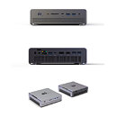
Qualcomm Snapdragon X Elite Mini-PC Dev Kit Arrives at $899

Qualcomm has started accepting preorders for its Snapdragon Dev Kit for Windows, based on the Snapdragon X Elite processor. Initially announced in May, the device is now available for preorder through Arrow at a competitive price point of $899. Despite its relatively high cost compared to typical mini PCs, it undercuts most recent laptops equipped with Snapdragon X processors, making it an attractive option for both developers and power users alike. Measuring a mere 199 x 175 x 35 mm, it comes equipped with 32 GB of LPDDR5x RAM, a 512 GB NVMe SSD, and support for the latest Wi-Fi 7 and Bluetooth 5 technologies. The connectivity options are equally robust, featuring three USB4 Type-C ports, two USB 3.2 Type-A ports, an HDMI output, and an Ethernet port.

This mini PC's heart lies the Snapdragon X Elite (X1E-00-1DE) processor. This chip houses 12 Oryon CPU cores capable of reaching speeds up to 3.8 GHz, with a dual-core boost potential of 4.3 GHz. The processor also integrates Adreno graphics, delivering up to 4.6 TFLOPS of performance, and a Hexagon NPU capable of up to 45 TOPS for AI tasks. While similar to its laptop counterpart, the X1E-84-100, this version is optimized for desktop use. It can consume up to 80 watts of power, enabling superior sustained performance without the constraints of battery life or heat dissipation typically associated with mobile devices. This dev kit is made primarily to optimize x86-64 software to run on the Arm platform; hence, removing the power limit is beneficial for translating the code to Windows on Arm. The Snapdragon Dev Kit for Windows ships with a 180 W power adapter and comes pre-installed with Windows 11, making it ready for immediate use upon arrival.

AMD Strix Point Silicon Pictured and Annotated

The first die shot of AMD's new 4 nm "Strix Point" mobile processor surfaced, thanks to an enthusiast on Chinese social media. "Strix Point" is a significantly larger die than "Phoenix." It measures 12.06 mm x 18.71 mm (L x W), compared to the 9.06 mm x 15.01 mm of "Phoenix." Much of this die size increase comes from the larger CPU, iGPU, and NPU. The process has been improved from TSMC N4 on "Phoenix" and its derivative "Hawk Point," to the newer TSMC N4P node.

Nemez (GPUsAreMagic) annotated the die shot in great detail. The CPU now has 12 cores spread across two CCX, one of which contains four "Zen 5" cores sharing a 16 MB L3 cache; and the other with eight "Zen 5c" cores sharing an 8 MB L3 cache. The two CCXs connect to the rest of the chip over Infinity Fabric. The rather large iGPU takes up the central region of the die. It is based on the RDNA 3.5 graphics architecture, and features 8 workgroup processors (WGPs), or 16 compute units (CU) worth 1,024 stream processors. Other key components include four render backends worth 16 ROPs, and control logic. The GPU has its own 2 MB of L2 cache that cushions transfers to the Infinity Fabric.

AMD Strix Point SoC Reintroduces Dual-CCX CPU, Other Interesting Silicon Details Revealed

Since its reveal last week, we got a slightly more technical deep-dive from AMD on its two upcoming processors—the "Strix Point" silicon powering its Ryzen AI 300 series mobile processors; and the "Granite Ridge" chiplet MCM powering its Ryzen 9000 desktop processors. We present a closer look into the "Strix Point" SoC in this article. It turns out that "Strix Point" takes a significantly different approach to heterogeneous multicore than "Phoenix 2." AMD gave us a close look at how this works. AMD built the "Strix Point" monolithic silicon on the TSMC N4P foundry node, with a die-area of around 232 mm².

The "Strix Point" silicon sees the company's Infinity Fabric interconnect as its omnipresent ether. This is a point-to-point interconnect, unlike the ringbus on some Intel processors. The main compute machinery on the "Strix Point" SoC are its two CPU compute complexes (CCX), each with a 32b (read)/16b (write) per cycle data-path to the fabric. The concept of CCX makes a comeback with "Strix Point" after nearly two generations of "Zen." The first CCX contains the chip's four full-sized "Zen 5" CPU cores, which share a 16 MB L3 cache among themselves. The second CCX contains the chip's eight "Zen 5c" cores that share a smaller 8 MB L3 cache. Each of the 12 cores has a 1 MB dedicated L2 cache.

AMD Details the Radeon 890M RDNA 3.5 iGPU of "Strix Point" a bit More

AMD presented a closer look at the Radeon 890M iGPU powering the Ryzen AI 300 series "Strix Point" mobile processor. The iGPU introduces the new RDNA 3.5 graphics architecture, with several architecture-level improvements built around the existing RDNA 3 SIMD, to yield performance/Watt improvements that AMD could trade in to increase the SIMD muscle for its processors, and proportionately increase performance. The iGPU features one Shader Engine with 8 workgroup processors (WGPs), which amount to 16 CU (compute units), for a total of 1,024 stream processors, 32 AI accelerators, and 16 Ray accelerators. The iGPU also has 4 render backends+, for 16 ROPs. It is specced with a maximum engine clock of 2.90 GHz, which yields over 11 TFLOP/s of FP32 throughput, which is around 30% higher than the iGPU of "Phoenix" (12 CU, RDNA 3), at comparable power.

AMD goes into the finer points of how it yielded the performance/Watt gains. The company worked on the texture subsystem to double the texture sampler rate, and introduced point-sampling acceleration. The shader sub-system features interpolation and comparison rate doubling. The raster sub-system introduces sub-batching of batch raster operations, with a programmable bin order, for the hardware to be more efficient. Lastly, AMD worked on the iGPU's memory-management, to be more aware of LPDDR5 (which has a different physical layer or way of writing/fetching than GDDR6). The company worked on improving the memory compression technologies, to improve performance, and reduce the iGPU's memory footprint.

Memory Industry Revenue Expected to Reach Record High in 2025 Due to Increasing Average Prices and the Rise of HBM and QLC

TrendForce's latest report on the memory industry reveals that DRAM and NAND Flash revenues are expected to see significant increases of 75% and 77%, respectively, in 2024, driven by increased bit demand, an improved supply-demand structure, and the rise of high-value products like HBM.

Furthermore, industry revenues are projected to continue growing in 2025, with DRAM expected to increase by 51% and NAND Flash by 29%, reaching record highs. This growth is anticipated to revive capital expenditures and boost demand for upstream raw materials, although it will also increase cost pressure for memory buyers.
Return to Keyword Browsing
Nov 18th, 2024 20:30 EST change timezone

New Forum Posts

Popular Reviews

Controversial News Posts