News Posts matching #LPDDR5

Return to Keyword Browsing

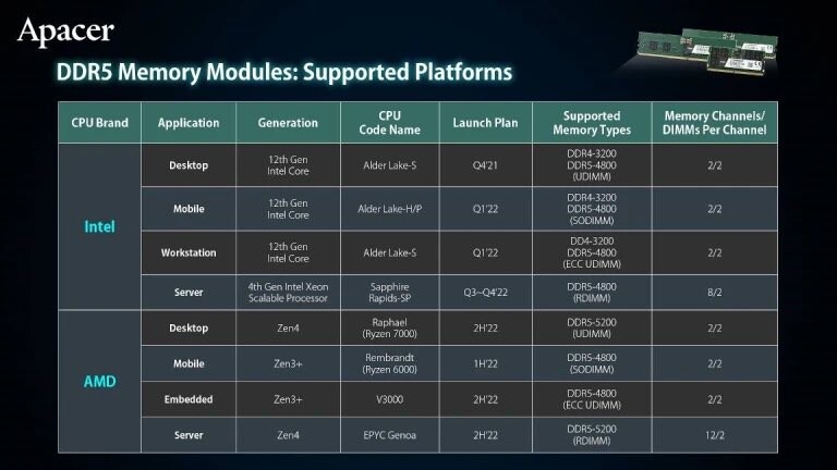
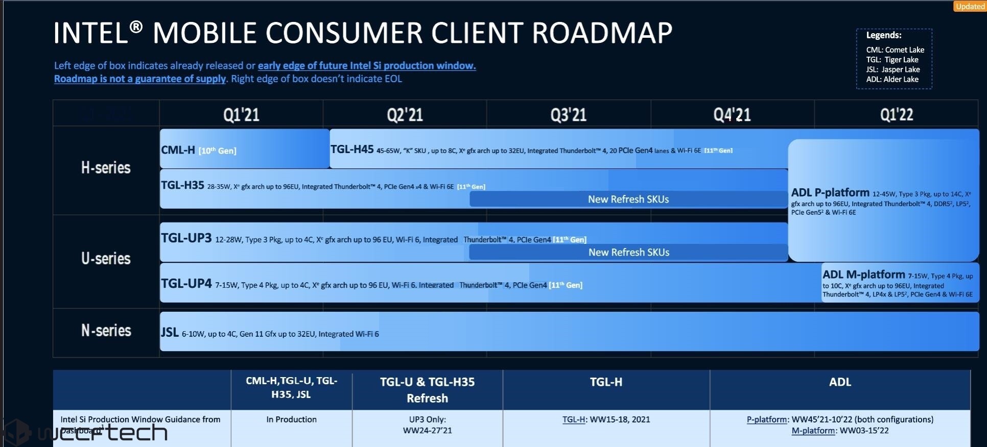
AMD Ryzen 7000 "Raphael" to Ship with DDR5-5200 Native Support

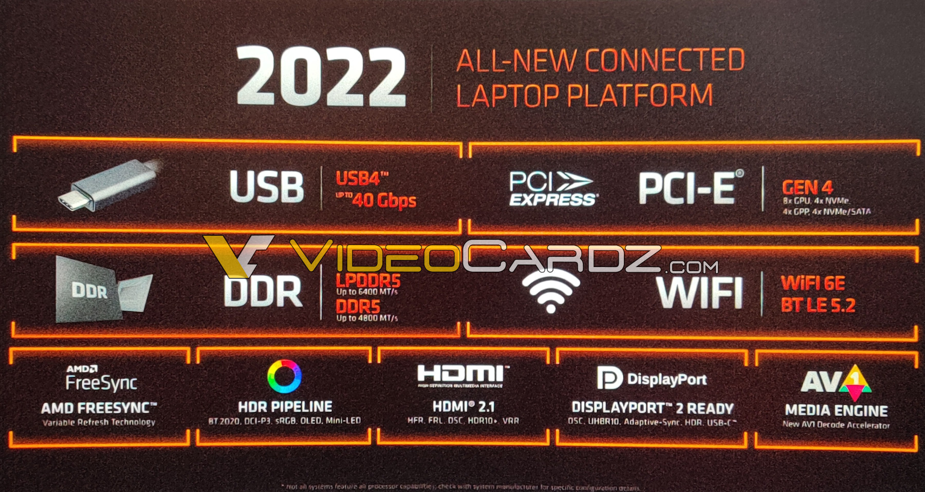
AMD's upcoming Socket AM5 Ryzen 7000-series "Raphael" desktop processors will ship with native support for DDR5-5200 memory speed, according to a marketing slide by memory maker Apacer (which also owns the overclocking memory brand ZADAK). The "Zen 4" based desktop processors will feature a dual-channel DDR5 (4 sub-channel) interface, just like the 12th Gen Core "Alder Lake," but with no backwards compatibility with DDR4.

AMD already stated that Ryzen 7000 processors have a design focus on memory overclocking capabilities, including AMD EXPO, a custom memory module SPD extension standard rivaling Intel XMP 3.0, which will come with fine-grained settings specific to the AMD memory controller architecture. Until now, AMD relied on A-XMP, a motherboard vendor-enabled feature based in the UEFI firmware setup program, which translates Intel XMP SPD profiles of memory modules into AMD-approximate settings.

NVIDIA Unveils Grace CPU Superchip with 144 Cores and 1 TB/s Bandwidth

NVIDIA has today announced its Grace CPU Superchip, a monstrous design focused on heavy HPC and AI processing workloads. Previously, team green has teased an in-house developed CPU that is supposed to go into servers and create an entirely new segment for the company. Today, we got a more detailed look at the plan with the Grace CPU Superchip. The Superchip package represents a package of two Grace processors, each containing 72 cores. These cores are based on Arm v9 in structure set architecture iteration and two CPUs total for 144 cores in the Superchip module. These cores are surrounded by a now unknown amount of LPDDR5x with ECC memory, running at 1 TB/s total bandwidth.

NVIDIA Grace CPU Superchip uses the NVLink-C2C cache coherent interconnect, which delivers 900 GB/s bandwidth, seven times more than the PCIe 5.0 protocol. The company targets two-fold performance per Watt improvement over today's CPUs and wants to bring efficiency and performance together. We have some preliminary benchmark information provided by NVIDIA. In the SPECrate2017_int_base integer benchmark, the Grace CPU Superchip scores over 740 points, which is just the simulation for now. This means that the performance target is not finalized yet, teasing a higher number in the future. The company expects to ship the Grace CPU Superchip in the first half of 2023, with an already supported ecosystem of software, including NVIDIA RTX, HPC, NVIDIA AI, and NVIDIA Omniverse software stacks and platforms.
NVIDIA Grace CPU Superchip

Apple Mac Studio Taken Apart, Reveals Giant M1 Ultra SoC

Max Tech performed the first detailed teardown of the Apple Mac Studio, the most powerful Mac since Apple dumped Intel for processors in favor of its own silicon based around high-performance Arm chips built from the ground-up for its own software ecosystem. The M1 Ultra SoC powering the Mac Studio is its most striking piece of technology, with Apple attaching some very tall performance claims not just for its CPU compute performance, but also graphics rendering performance.

The M1 Ultra SoC is physically huge, with roughly similar package size to an AMD EPYC processor in the SP3 package. An integrated heatspreader (IHS) covers almost the entire topside of the package. Things get interesting under the hood. The M1 Ultra is a multi-chip module of two M1 Max dies connected on package using Apple UltraFusion, a coherent fabric interconnect that allows the various components of the two M1 Max dies to access memory controlled by the other die. Speaking of memory, The M1 Ultra features up to 128 GB of LPDDR5 memory that's on-package, This memory is used for the CPU, GPU, as well as the neural processor, and has a combined memory bandwidth of 800 GB/s. The M1 Ultra features up to 20 CPU cores, up to 32 Neural cores, and up to 64 GPU cores (8,192 programmable shaders).

Intel Arc GPU Found Inside Samsung Galaxy Book2 Pro is now Selling for $1350

Intel's Arc discrete lineup of graphics card are set to hit the notebook/laptop segment first, and today's discovery is no different. BHPhotoVideo, one of the largest US tech retailers, has posted a listing of Samsung's Galaxy Book2 Pro laptop, spotting Intel's Arc discrete graphics solution. According to the listing, this model was spotting an undisclosed Intel Arc Graphics, 2.1 GHz 12-core CPU, 16 GB of LPDDR5-6400 memory, 512 GB of NVMe PCIe Gen4 storage, 15.6-inch 1080p AMOLED display, WiFi-6E, and came in just 1.13 KG body weight. All of this is packed at 1349.99 USD, which is an early sign of the structure of laptop prices carrying Intel's Arc GPUs.

BHPhotoVideo has now taken down the website listing; however, we still have evidence thanks to the leaker, which you can see below. For more information regarding the exact SKU and more Arc Alchemist data, we have to wait for the March 30th launch.

Dynabook Unveils Three New Portégé Laptops with12th Gen Core Processors and vPro, Thunderbolt Dock

Dynabook Americas, Inc., formerly Toshiba PC Company, today announced the all-new Portégé X40L-K, a hyperlight 14-inch modern laptop that takes premium, high-performance computing to new extremes. The Portégé X40L-K is among the first wave of new laptops from Dynabook to benefit from the enhanced performance, efficiency and security offered by hybrid architecture 12th Gen Intel Core P-Series 28 W processors, LPDDR5 memory and Windows 11 Pro.

"The all-new Intel Evo based Portégé X40L-K is truly a masterpiece every way you look at it and serves as an impressive demonstration of Dynabook's nearly four decades of experience in engineering premium laptops for mobile professionals," said James Robbins, General Manager, Dynabook Americas, Inc. "It's compact, powerful, durable, uniquely stylish, and secure. While all impressive, none of these qualities sum up the magic of this laptop. You must hold it to truly appreciate the incredible engineering and craftsmanship that went into making it the lightest and highest-performing 14-inch laptop in our history."

Acer Announces the New Swift 5, a Powerful and Premium Ultraportable Laptop

Acer today updated its popular Swift line of notebooks with new models of the Swift 5 and Swift 3. To push the limits of what's possible with a thin and light device, these new laptops come with 12th Gen Intel Core processors, gorgeous touchscreen displays, and all-day battery life: everything a mobile professional needs.

"Designed for executives and mobile professionals, the latest Acer Swift 5 offers a perfect balance of performance and portability," said James Lin, General Manager, Notebooks, IT Products Business, Acer. "The Intel Evo-verified laptop not only provides a great experience, it is housed in a stylish thin-and-light CNC-machined unibody chassis featuring a gorgeous touchscreen display." "Intel and Acer have a long history of co-engineering to deliver amazing laptops," said Josh Newman, VP and GM of Client Computing Group Mobile Innovation. "Now, more than ever, our engineers are focused on the experiences that matter most with the Intel Evo platform, powered by 12th Gen Intel Core processors."

Intel Announces 12th Gen Core "Alder Lake" Mobile Processors and Evo Third Edition

Today, Intel expands the 12th Gen Intel Core mobile processor lineup with the official launch of 12th Gen Intel Core P-series and U-series processors. Engineered for blazing performance and superior productivity, these 20 new mobile processors will power the next generation of thin-and-light laptops. The first devices will be available in March 2022, with more than 250 coming this year from Acer, Asus, Dell, Fujitsu, HP, Lenovo, LG, MSI, NEC, Samsung and others.

"Following our launch of the fastest mobile processor for gaming, we're now expanding our 12th Gen Intel Core processor family to deliver a massive leap forward in performance for thin-and-light laptops. From the ultra-thin form factors to enthusiast-grade performance in a sleek design, we're providing consumers and businesses with leadership performance and cutting-edge technologies."

JEDEC Publishes HBM3 Update to High Bandwidth Memory (HBM) Standard

JEDEC Solid State Technology Association, the global leader in the development of standards for the microelectronics industry, today announced the publication of the next version of its High Bandwidth Memory (HBM) DRAM standard: JESD238 HBM3, available for download from the JEDEC website. HBM3 is an innovative approach to raising the data processing rate used in applications where higher bandwidth, lower power consumption and capacity per area are essential to a solution's market success, including graphics processing and high-performance computing and servers.

Lenovo's ThinkBook Plus Gen 3 Features 120Hz 3072x1440 17.3-inch Display

We've already seen some leaked pictures of Lenovo's awkwardly named ThinkBook Plus Gen 3, but what they didn't convey was the specs and almost all of them are quite impressive. The main display might be the most impressive part, as it's a 17.3-inch, 120 Hz 16:10 panel with a resolution of 3072x1440, which is as far as we know, the first of its kind. Then there's the "tablet" which measures 8-inches, although it's fairly low resolution at 1280x800. It comes with a "digital pen" as Lenovo calls it and is designed for graphics works courtesy of a software plugin that allows it to work with Pantone colours.

CPU wise, we're looking at the brand new 12th gen Intel Core H-series of CPUs, although no mention of the exact SKUs was offered. There's support for up to 32 GB of LPDDR5 RAM and 2 TB of storage. Sadly, graphics are limited to the Intel Iris Xe GPU built into the CPU, which means it might not be the ideal notebook for some of the types of work it was intended for.

Intel Engineers Fastest Mobile Processor Ever with 12th Gen Intel Core Mobile

Today at CES 2022, Intel announced the world's fastest mobile processor, bringing its performance hybrid architecture to mobile platforms for the first time with new 12th Gen Intel Core mobile processors that are up to 40 percent faster than the previous generation mobile processor. Intel introduced 28 new 12th Gen Intel Core mobile processors that deliver a feature-rich suite of capabilities to create laptops for people to compute whenever and wherever they need - without compromise.

With the introduction of the full 12th Gen Intel Core desktop processor lineup, the 12th Gen Intel Core processor family also represents the company's most scalable lineup to date, powering designs across consumer, enterprise, the Internet of Things (IoT) and other applications. "Intel's new performance hybrid architecture is helping to accelerate the pace of innovation and the future of compute," said Gregory Bryant, executive vice president and general manager of Intel's Client Computing Group. "And, with the introduction of 12th Gen Intel Core mobile processors, we are unlocking new experiences and setting the standard of performance with the fastest processor for a laptop—ever."

AMD Ryzen 6000 "Rembrandt" Mobile Processors Pack Next-Gen Connectivity: Leak

AMD is planning to crash Intel's big 12th Gen Core "Alder Lake-P" mobile processor launch with its own next-gen launch, the Ryzen 6000 mobile processor series. These chips are the company's first built on the TSMC N6 (6 nm) silicon fabrication process, and combine up to 8 "Zen 3+" CPU cores, with a next-generation iGPU based on the RDNA2 graphics architecture. The company has given the Media CoreNext and Video CoreNext engines incremental updates, according to a leaked slide scored by VideoCardz.

Ryzen 6000 "Rembrandt" processors come with hardware-accelerated decode of the AV1 video format. The Display CoreNext (display I/O engine) now supports DisplayPort 2.0, complete with DSC, UHBR10, HDR10+, and variable refresh-rate. The HDR pipeline has awareness for the various display panel types, including OLED and mini-LED. The iGPU on "Rembrandt" features up to 12 compute units (768 stream processors). It remains to be seen if Ray Accelerators are featured, as that would make this the first iGPU (on the PC platform) with DirectX 12 Ultimate support.

Huawei Prepares Laptop Powered by Custom Kirin 5 nm SoC and DDR5 Memory

China's technology reliance on 3rd party companies seems to be getting smaller. One of the leading technology companies in China, Huawei, has designed a laptop powered by a custom 5 nm Kirin SoC with DDR5 memory. Called the Dyna Cloud L420, Huawei has prepared this model for the Chinese market to provide a fully functional laptop that will get the job done, with no risk of the potential security backdoors implemented in the processor. Powered by a brand new Kirin 9006C SoC manufactured on TSMC's 5 nm process, it features eight unknown cores running at 3.1 GHz frequency. We assume that those are custom cores designed by Huawei. This SoC is accompanied by 8 GB of LPDDR5 memory, with 256 GB and 512 GB UFS 3.1 configurations storage options.

When it comes to the rest of the laptop, it rocks a 14-inch 2160x1440 display. I/O options are solid as well, as this machine has an HDMI video output, two USB-A, one USB-C, and Gigabit Ethernet using a mini-RJ45 port. Connectivity is provided by Wi-Fi 6 and Bluetooth 4.2. There is a 56 W/h battery that provides the juice to keep it running when it comes to the battery. And to complete all of that, this laptop officially only supports Huawei's proprietary Kirin OS (KOS) and Unity OS (UOS), with expected support for HarmonyOS in the future. Pricing and availability information is a mistery at the present date.

Samsung Talks DDR6-12800, GDDR7 Development, and HBM3 Volume Production

During Samsung's Tech Day 2021, the company presented some interesting insights about the future of system memory technologies and how it plans to execute its production. Starting with the latest DDR5 standard, the company intends to follow JEDEC documents and offer some overclocking modules that surpass the specification advised by JEDEC. While the DDR5 standard specifies memory modules with 6,400 MT/s, Samsung will develop modules capable of overclocking up to 8,400 MT/s. These are not yet confirmed as they are still in the development phase. However, we can expect to see them in the later life of DDR5 memory.

The company also talked about the DDR6 standard, which is supposedly twice as fast as DDR5. The new DDR6 standard is still in early development, and all we know so far is that the number of memory channels per module is seeing a twofold increase over DDR5 to four channels. The number of memory banks also increases to 64. In addition to DDR6 for desktop and server use cases, the company is also working on Low Power DDR6 (LPDDR6) for mobile applications. While the company's LPDDR5 memory goes into volume production using the 1a-nm process at the beginning of 2022, the LPDDR6 is still in early development. The base speed for DDR6 modules will allegedly arrive at 12,800 MT/s, while overclocking modules will join the party at up to 17,000 MT/s. Mobile-oriented LPDDR6 version is also supposed to come with up to 17,000 MT/s speeds.

SK hynix Receives ISO 26262 FSM Certification

SK hynix announced that it has received an ISO 26262: 2018 FSM (Functional Safety Management) certification, the international standard for functional safety in automotive semiconductors. The global automotive functional safety certification institute, TUV Nord, conducted the assessment. Both companies commemorated the distinction by hosting an online ceremony. In attendance at the ceremony were Daeyong Shim, Head of Automotive Business, and Junho Song, Head of Quality System, from SK hynix and Bianca Pfuff, Profit Center Manager Functional Safety and Deputy Head of Certification Body SEECERT, and Josef Neumann, Senior Project Manager Functional Safety, from TUV Nord.

The ISO 26262 is the international standard for automobile functional safety established by the International Organization for Standardization (ISO) in 2011 to prevent accidents caused by automotive electrical and electronic systems failures. This certification awarded to SK hynix, ISO 26262: 2018, is the latest version with additional requirements for automotive semiconductors. In the automotive industry, safety, quality, and reliability are paramount. Therefore, it is becoming essential that producers of car electronic device related to safety meet ISO 26262 standards.

Synopsys Accelerates Multi-Die Designs with Industry's First Complete HBM3 IP and Verification Solutions

Synopsys, Inc. today announced the industry's first complete HBM3 IP solution, including controller, PHY, and verification IP for 2.5D multi-die package systems. HBM3 technology helps designers meet essential high-bandwidth and low-power memory requirements for system-on-chip (SoC) designs targeting high-performance computing, AI and graphics applications. Synopsys' DesignWare HBM3 Controller and PHY IP, built on silicon-proven HBM2E IP, leverage Synopsys' interposer expertise to provide a low-risk solution that enables high memory bandwidth at up to 921 GB/s.

The Synopsys verification solution, including Verification IP with built-in coverage and verification plans, off-the-shelf HBM3 memory models for ZeBu emulation, and HAPS prototyping system, accelerates verification from HBM3 IP to SoCs. To accelerate development of HBM3 system designs, Synopsys' 3DIC Compiler multi-die design platform provides a fully integrated architectural exploration, implementation and system-level analysis solution.

Intel Alder Lake-P Appears in Leaked Roadmap Featuring DDR5 & PCIe 5.0 Support

Intel is expected to announce their desktop Alder Lake processors later this month on October 28th and it would appear that laptop processors could enter production as early as November. These revelations come from a leaked roadmap published by Wccftech that lists the Alder Lake-P and Alder Lake-M processor families for launch in Q4 2021 and Q1 2022 respectively. The production window for Alder Lake-P opens November 8th and closes March 13th while for Alder Lake-M that period is from January 17th to April 17th.

The roadmap lists Alder Lake-P processors as featuring a TDP between 12 W to 45 W and Alder Lake-M covering 7 W to 15 W. The two platforms will both feature up to 96 Xe graphics Execution units along with Thunderbolt 4 and WiFi 6E connectivity. Alder Lake-P will include PCIe 5.0 and DDR5 support with no mention of DDR4 compatibility while Alder Lake-M will get PCIe 4.0 and LPDDR4X/LPDDR5. The mobile lineup is divided into 3 groups of which the flagship H55 was not mentioned in the roadmap indicating a post Q1 2022 release.

Samsung Brings In-memory Processing Power to Wider Range of Applications

Samsung Electronics the world leader in advanced memory technology, today showcased its latest advancements with processing-in-memory (PIM) technology at Hot Chips 33—a leading semiconductor conference where the most notable microprocessor and IC innovations are unveiled each year. Samsung's revelations include the first successful integration of its PIM-enabled High Bandwidth Memory (HBM-PIM) into a commercialized accelerator system, and broadened PIM applications to embrace DRAM modules and mobile memory, in accelerating the move toward the convergence of memory and logic.

In February, Samsung introduced the industry's first HBM-PIM (Aquabolt-XL), which incorporates the AI processing function into Samsung's HBM2 Aquabolt, to enhance high-speed data processing in supercomputers and AI applications. The HBM-PIM has since been tested in the Xilinx Virtex Ultrascale+ (Alveo) AI accelerator, where it delivered an almost 2.5X system performance gain as well as more than a 60% cut in energy consumption.

MediaTek Announces Dimensity 920 and Dimensity 810 Chips for 5G Smartphones

MediaTek today announced the new Dimensity 920 and Dimensity 810 chipsets, the latest additions to its Dimensity 5G family. This debut gives smartphone makers the ability to provide boosted performance, brilliant imaging and smarter displays to their customers.

Designed for powerful 5G smartphones, the Dimensity 920 balances performance, power and cost to provide an incredible mobile experience. Built using the 6nm high-performance manufacturing node, it supports intelligent displays and hardware-based 4K HDR video capture, while also offering a 9% boost in gaming performance compared to its predecessor, the Dimensity 900.

JEDEC Publishes the New LPDDR5X Memory Standard

JEDEC Solid State Technology Association, the global leader in standards development for the microelectronics industry, today announced the publication of JESD209-5B, Low Power Double Data Rate 5 (LPDDR5). JESD209-5B includes both an update to the LPDDR5 standard that is focused on improving performance, power and flexibility, and a new LPDDR5X standard, which is an optional extension to LPDDR5.

Taken together, LPDDR5 and LPDDR5X are designed to significantly boost memory speed and efficiency for a variety of uses including mobile devices, such as 5G smartphones and artificial intelligence (AI) applications. Developed by JEDEC's JC-42.6 Subcommittee for Low Power Memories, JESD209-5B is available for download from the JEDEC website.

Valve Steam Deck SoC Detailed: AMD Brings Zen2 and RDNA2 to the Table

Valve today announced its first big splash into the console market with Steam Deck, a device out to eat the Nintendo Switch's lunch. The announcement comes as yet another feather in AMD's cap for its semi-custom SoC business, benefiting from being the only company with an x86-64 CPU license and having a cutting-edge graphics hardware IP. Built on the 7 nm node at TSMC, the semi-custom chip at the heart of the Steam Deck is designed for extended gameplay on battery, and is a monolithic silicon that combines CPU, GPU, and core-logic.

The yet-unnamed semi-custom chip features a 4-core/8-thread CPU based on the "Zen 2" microarchitecture, with a nominal clock speed of 2.40 GHz, and up to 3.50 GHz boost. The CPU component offers an FP32 throughput of 448 GFLOP/s. The GPU is based on AMD's latest RDNA2 graphics architecture—the same one powering the Xbox Series X, PlayStation 5, and Radeon RX 6900 XT—and is comprised of 8 RDNA2 compute units (512 stream processors). The GPU operates at an engine clock speed of 1.10 GHz to 1.60 GHz, with peak compute power of 1.6 TFLOP/s. The silicon uses a unified memory interface, and a cutting-edge LPDDR5 memory controller.

Surface Pro X with Windows 11 Shown Running Microsoft-branded Qualcomm Arm SoC

A next-generation Microsoft Surface Pro X with Windows 11 was shown running a Microsoft-branded processor that's expected to be a design collaboration between the company and Qualcomm, in a bid to develop a high performance/Watt solution rivaling the Apple M1. Microsoft's contribution to this is the x86-64 emulation heavily integrated into Windows 11, letting you run native x86-64 apps seamlessly, with the OS handling the hardware abstraction much like WOW64.

Called the Microsoft SQ2, the silicon features an 8-core/8-thread CPU, and an iGPU that meets the minimum requirements of Windows 11 for its standard UI, with just enough power for web-browsing with high-res videos. The CPU runs at speeds of up to 3.15 GHz, and has a fairly advanced memory system that includes a 3-level cache and LPDDR5 memory.

Samsung Brings Flagship Features to Broader Smartphone Market with LPDDR5 Multichip Package

Samsung Electronics Co., Ltd., the world leader in advanced memory technology, today announced that it has begun mass producing its latest smartphone memory solution, the LPDDR5 UFS-based multichip package (uMCP). Samsung's uMCP integrates the fastest LPDDR5 DRAM with the latest UFS 3.1 NAND flash, delivering flagship-level performance to a much broader range of smartphone users.

"Samsung's new LPDDR5 uMCP is built upon our rich legacy of memory advancements and packaging know-how, enabling consumers to enjoy uninterrupted streaming, gaming and mixed reality experiences even in lower-tier devices," said Young-soo Sohn, vice president of the Memory Product Planning Team at Samsung Electronics. "As 5G-compatible devices become more mainstream, we anticipate that our latest multichip package innovation will accelerate the market transition to 5G and beyond, and help to bring the metaverse into our everyday lives a lot faster."

MediaTek Announces New 6nm Dimensity 900 5G Chipset

MediaTek today announced the new Dimensity 900 5G chipset, the latest addition to its Dimensity 5G family. The Dimensity 900 chipset, built on the 6nm high-performance manufacturing node, supports Wi-Fi 6 connectivity, ultra-fast FHD+ 120Hz displays and a 108MP main camera for an all-around incredible experience. "Dimensity 900 brings a suite of connectivity, display and 4K HDR visual enhancements to high-tier 5G smartphones and gives brands great design flexibility for their 5G portfolios," said Dr. JC Hsu, Corporate VP and GM of MediaTek's Wireless Communications Business Unit. "The chipset's support for 5G and Wi-Fi 6 ensures users get the most of out their devices with super-fast and reliable connectivity."

The Dimensity 900 chipset is integrated with a 5G New Radio (NR) sub-6GHz modem with carrier aggregation and support for bandwidth up to 120 MHz. The chipset is equipped with an 8-core central processing unit (CPU) consisting of two Arm Cortex-A78 processors with a clock speed of up to 2.4 GHz and six Arm Cortex-A55 cores operating at up to 2.00 GHz. Dimensity 900 supports flagship LPDDR5 memory and UFS 3.1 storage, and can adapt to a 120 Hz screen refresh rate, bringing excellent performance improvements and a seamless experience to 5G mobile devices.

NVIDIA Announces Grace CPU for Giant AI and High Performance Computing Workloads

NVIDIA today announced its first data center CPU, an Arm-based processor that will deliver 10x the performance of today's fastest servers on the most complex AI and high performance computing workloads.

The result of more than 10,000 engineering years of work, the NVIDIA Grace CPU is designed to address the computing requirements for the world's most advanced applications—including natural language processing, recommender systems and AI supercomputing—that analyze enormous datasets requiring both ultra-fast compute performance and massive memory. It combines energy-efficient Arm CPU cores with an innovative low-power memory subsystem to deliver high performance with great efficiency.

SK Hynix Begins Mass-Production of 18-Gigabyte LPDDR5 Mobile DRAM Chips

SK hynix Inc announced that it has started mass-production of 18 GB (gigabyte) LPDDR5 mobile DRAM, which offers the largest capacity in the industry. This product will be equipped in premium smartphones to support an optimal environment for games with high resolution image and also high quality videos. SK hynix also expects that application will continue expanding to include the latest technologies, including ultra-high-performance camera applications and artificial intelligence (AI).

"This product will improve the processing speed and image quality by expanding the data temporary storage space, as the capacity increases compared to the previous 16 GB product," an official from the company said. The new product runs at up to 6,400 Mbps (megabits-per-second), around 20% faster than the mobile DRAM (LPDDR5 with 5,500 Mbps) for existing smartphones, a data rate that is capable of transferring ten 5 GB FHD (Full-HD) movies per second.
Return to Keyword Browsing
Jul 5th, 2025 12:44 CDT change timezone

New Forum Posts

Popular Reviews

TPU on YouTube

Controversial News Posts