Tuesday, April 28th 2020
Researchers Propose New Density Metric for Semiconductor Technology
In today's world, fabrication process identification of semiconductor technology has become little more than marketing fluff. Whereas not that long ago, fabrication processes could (mostly) be directly compared on the basis of transistor density (ie, 300 nm, 32 nm, 14 nm, and now 7 nm), recent advances in manufacturing technologies and their end terminology have lost all significance when it comes to actually describe how density that process is. The way manufacturers measured this semiconductor density used to directly refer to the minimum gate length in transistors fabricated in a given process - that, is, in 300 nm, the minimum gate length that could be achieved was 300 nanometers, in 32 nm, 32 nanometres, and so on. As of now, that isn't happening - which is why we've got Intel saying that its 10 nm fabrication process will be comparable to TSMC's current 7 nm process.
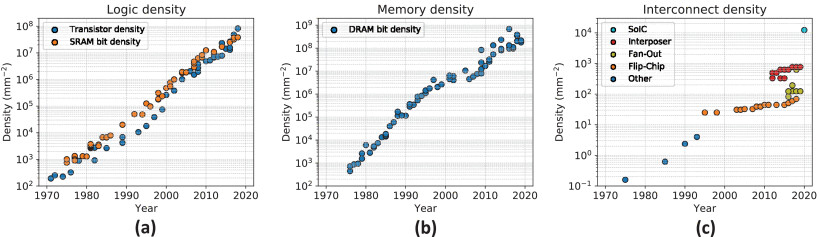
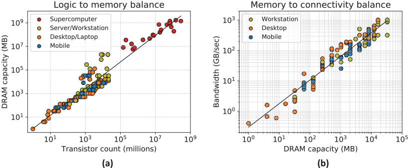
This leads to a number of difficulties for interested parties to actually glean any meaningful information from this particular semiconductor metric alone. Now, a team of researchers has tackled this problem by suggesting a different way to express semiconductor manufacturing capability. Their intention is to allow to "gauge advances in future generations of semiconductor technologies in a holistic way, by accounting for the progress in logic, memory, and packaging/integration technologies simultaneously." As such, their proposed density metric follows a [DL, DM, DC] philosophy, where DL is the density of logic transistors (in #/mm²), DM is the bit density of main memory (currently the off-chip DRAM density, in #/mm²), and DC is the density of connections between the main memory and logic (in #/mm²). The researchers say that current top semiconductor technology density available would be described by this system as [38M, 383M, 12K].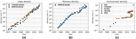 The researchers include metrics such as DM and DC because current computer systems absolutely depend on off-chip memory density, and I/O and actual logic/memory throughput is increasingly important in all computing scenarios (and especially as computing performance increases). Furthermore, the researchers have noted a comparable increase in density of logic transistors and DRAM bit density, which adds to this new density metric. Remember that these values are supposed to represent the maximum effective capability of any given manufacturing process - this means that a next-generation process from Intel could include maximum transistor density expressed in the result of an equation as simple as number of transistors divided by the die area; the maximum available DRAM bit density of memory that can be paired with this fabrication process chip (we expect this number to be changed across product portfolios in a given generation should compatible DRAM density advancements occur in the lifetime of a given die logic manufacturing lifetime; as well as density of logic-to-memory connectivity.
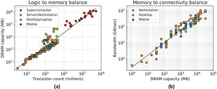 Considering the current naming convention landscape for manufacturing process density is... filled with as many plot-holes as some super-hero franchises, this seems like a sensible way to go about in actually forcing a level playing field between manufacturers. They keep their leeway in marketing terms to describe their processes as they want, but must also provide these density metrics for their process technologies. And since this refers to the maximum densities their process can support (when it comes to transistor logic and memory connection logic densities), it ensures that consumers, institutions, and companies can actually look at the semiconductor landscape with a clear picture.
Source:
IEEE Explore
This leads to a number of difficulties for interested parties to actually glean any meaningful information from this particular semiconductor metric alone. Now, a team of researchers has tackled this problem by suggesting a different way to express semiconductor manufacturing capability. Their intention is to allow to "gauge advances in future generations of semiconductor technologies in a holistic way, by accounting for the progress in logic, memory, and packaging/integration technologies simultaneously." As such, their proposed density metric follows a [DL, DM, DC] philosophy, where DL is the density of logic transistors (in #/mm²), DM is the bit density of main memory (currently the off-chip DRAM density, in #/mm²), and DC is the density of connections between the main memory and logic (in #/mm²). The researchers say that current top semiconductor technology density available would be described by this system as [38M, 383M, 12K].
15 Comments on Researchers Propose New Density Metric for Semiconductor Technology
IEEE should handle this.
To give example, you can have (relatively) low-power / low-performance builds - like phone SoCs use - and get one density, use the same process tech with different 'toolkits' for high-power / high performance designs and wind up with very very different densities. Also the type of design matters a lot, you can get very high density on something like SRAM or NAND and then wind up with poor density doing logic circuits.
And it gets a whole lot more complex than that. They probably need two different ratings with a category qualifier, one for simple repetitive designs like RAM/NAND, and another for complex gates. So you might have a rating that looks like 7N/16N/HP for a high-power/performance toolkit on a node that can achieve 7nm with RAM/NAND and 16nm with gate logic. This is what I suspect TSMC 1st gen 7nm would look like, as actual achieved transistor density from their '7nm' is not much better than Intel 14nm.
Once you know that, it goes a long way to understanding why it wasn't until 7nm that AMDs 7nm based products actually matched up well against Intel 14nm. TSMC 7NP (7+) does look to be better than Intel 14N(++++). Point being the current published process node numbers are 70% marketing.
*things = whole, working transistors
Yeah raw density is one thing but that measures the chip, not the node.
This stuff belongs to tech sheets, not press.