Tuesday, June 30th 2020

Microsoft Rumored To Release Budget Xbox Series S Console

In a recent report by the Verge, Microsoft is reportedly planning a budget console to go along with the Xbox Series X known as the Xbox Series S. The Xbox Series S will be a successor to the popular Xbox One S, codenamed Lockhart it's set to feature the key next-generation improvements found in the Xbox Series X and provide them at a lower price point.

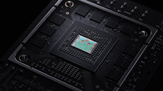
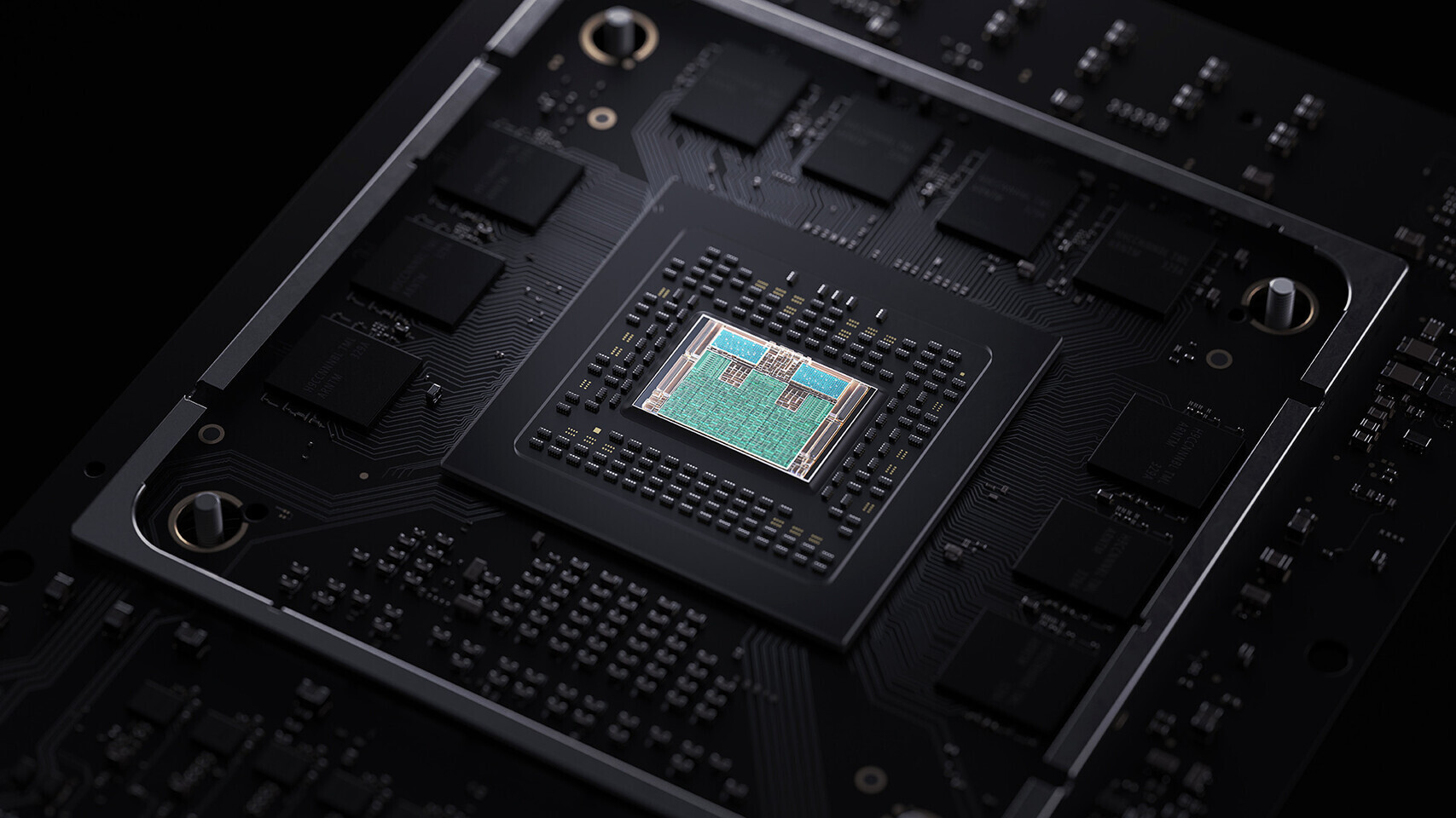
Sources say that the Xbox Series S will target 1080p 60FPS and 1440p 6̶0̶F̶P̶S̶ 30FPS gaming performance, this will be achieved with roughly 1/3rd of the GPU power at 4 TeraFLOPs, and 10 GB of GDDR6 RAM. The Xbox Series S console is rumored to share the same 7 nm AMD Zen 2 SoC a̶t̶ ̶a̶ ̶l̶o̶w̶e̶r̶ ̶c̶l̶o̶c̶k̶ and the same ultra-fast PCIe 4.0 SSD. The console may not feature a disc drive like the Xbox One S All Digital Edition. Microsoft is yet to publicly say anything about the console, so take these rumors with a grain of salt.

Update Jun 30th: Sources tell Eurogamer that Microsoft is planning to unveil the console at an event in August.
Sources: The Verge, @tomwarren, Eurogamer
Add your own comment

57 Comments on Microsoft Rumored To Release Budget Xbox Series S Console

#51
Valantar
NaitoI understand that. However, 4K TVs have become very prevalent (I've seen as low as $300 where I am) and for a console which will probably be in the market for 7 to 8 years, it should still be able to drive 4K at least as well as the Scorpio (One X) currently does. Scaling back performance to only support 1080/1440p seems short sighted. Though, as others have pointed out, 4TF of RDNA2 may perform as well or better than the 6TF on hand in the Scorpio.
I would assume it would support 4k output but render games at a maximum resolution of 1080p or 1440p, with upscaling to make up the difference. For a huge swathe of the public - such as the millions buying consoles to play the most recent Fifa or Madden - this would likely be entirely sufficient for their wants and needs. I would also assume it to play any Xbox One title at settings, resolutions and framerates matching the XOX.
Posted on Reply
#52
danbert2000
demian_viSwitch Lite showed that there's a market for cheaper versions of consoles. not everyone has a 4k tv and someone who can't afford a 4k tv, would likely prefer a cheaper console.
Microsoft has definitely done some market research before deciding this


Cpu will be the same.
CPU portion will be the same, but it's all the same chip. GPU portion of the overall APU will either be smaller (cost savings from smaller dies, which means more per wafer) or harvested (meaning that they are the same physical chip as the Series X, but defective in several regions which are then deactivated physically with laser cuts). The latter has cost savings from reusing chips that would have been thrown away, so as long as the defective chips meet demand they are essentially free. If not, they would likely have to start cutting perfectly good Series X chips to meet the lower price point.

My bet is in the beginning it will be harvested defective Series X dies, and once the 7 nm fab defect rate drops, they'll have a custom chip to go along with a fab shrink. Best of both worlds and in the beginning you're just managing one chip run.
Posted on Reply
#53
Valantar
danbert2000CPU portion will be the same, but it's all the same chip. GPU portion of the overall APU will either be smaller (cost savings from smaller dies, which means more per wafer) or harvested (meaning that they are the same physical chip as the Series X, but defective in several regions which are then deactivated physically with laser cuts). The latter has cost savings from reusing chips that would have been thrown away, so as long as the defective chips meet demand they are essentially free. If not, they would likely have to start cutting perfectly good Series X chips to meet the lower price point.

My bet is in the beginning it will be harvested defective Series X dies, and once the 7 nm fab defect rate drops, they'll have a custom chip to go along with a fab shrink. Best of both worlds and in the beginning you're just managing one chip run.
Given that TSMC 7nm is now a mature node and the XSX die has four CUs spare and is a relatively reasonable die size (bigger, but still comparable to a Navi 10), I see no reason to expect there to be any noticeable defect rate for those chips - at least not ones that can be harvested. Given what consumes the most die area it's reasonable to expect most errors to happen in the GPU, where there can then be up to four errors per die, all in different CUs (highly unlikely) before the chip fails to pass muster. If there's a flaw in the CPU or something else that's shared, they can't harvest it anyhow.
Posted on Reply
#54
demian_vi
ValantarCPU being the same does not mean the SoC is the same, and it's highly unlikely that there will be enough defective XSX dice to support this being based on cut down chips. If this is real it's likely a second die design with the same CPU but less GPU CUs and RAM channels.
Cpu is the same and gpu is different. I never said anything about the Soc, we already know it's different.
Posted on Reply
#55
Valantar
demian_viCpu is the same and gpu is different. I never said anything about the Soc, we already know it's different.
I didn't say that you said that, I just pointed out that the CPU being the same is a relatively small factor in the overall SoC design, and that other factors point in the direction of a separate die.
Posted on Reply
#56
danbert2000
ValantarGiven that TSMC 7nm is now a mature node and the XSX die has four CUs spare and is a relatively reasonable die size (bigger, but still comparable to a Navi 10), I see no reason to expect there to be any noticeable defect rate for those chips - at least not ones that can be harvested. Given what consumes the most die area it's reasonable to expect most errors to happen in the GPU, where there can then be up to four errors per die, all in different CUs (highly unlikely) before the chip fails to pass muster. If there's a flaw in the CPU or something else that's shared, they can't harvest it anyhow.
Just because it's a mature node doesn't mean there isn't defect rates. It means that the defect rates are acceptable and making the chips is reliably profitable. That could mean that the wafer cost goes down or the defect rate goes down, but it can never be zero defects, especially at the edge of the wafer. Nvidia and AMD harvest defective dies for their lower end GPUs all the time, and Nvidia especially is on a very mature node at this point and still has the cost structure set up to make few different chips with cut resources. Intel has defective chips on 14 nm after all this time on it. Still, we don't have any information at this point about whether the Series S chips will be new or harvested, but my bet is in the beginning they will be harvested so Microsoft can reuse some of those very large APUs that have just a few defects in the GPU portion.
Posted on Reply
#57
Valantar
danbert2000Just because it's a mature node doesn't mean there isn't defect rates. It means that the defect rates are acceptable and making the chips is reliably profitable. That could mean that the wafer cost goes down or the defect rate goes down, but it can never be zero defects, especially at the edge of the wafer. Nvidia and AMD harvest defective dies for their lower end GPUs all the time, and Nvidia especially is on a very mature node at this point and still has the cost structure set up to make few different chips with cut resources. Intel has defective chips on 14 nm after all this time on it. Still, we don't have any information at this point about whether the Series S chips will be new or harvested, but my bet is in the beginning they will be harvested so Microsoft can reuse some of those very large APUs that have just a few defects in the GPU portion.
Seriously, did you even read the post you quoted? Did I ever say that there were no errors on TSMC 7nm? Not even close. I said that it is a mature node, which implies a low but obviously not nonexistent error rate (no node has ever been free of errors). I also said that the GPU part of the SoC has four CUs more than necessary to allow for up to four distributed defects per die without needing to discard it (as long as they are all in the GPU, which isn't unlikely given that it occupies the vast majority of the die). Four is more than zero, right? What I said was that with currently publicized error rates for TSMC 7nm (which IIRC were quoted here earlier; you can easily plug them into a wafer yield calculator if you want) the chances of a single die having more than four errors on a single die are essentially zero - especially considering that if even one of those errors is in a part with no redundancy (such as the CPU cores or I/O) the die wouldn't be harvestable for a lower end console anyhow.
Posted on Reply
Add your own comment
Jul 31st, 2024 17:20 EDT change timezone

New Forum Posts

Popular Reviews

Controversial News Posts