Report an Error


AMD Capsaicin
Capsaicin
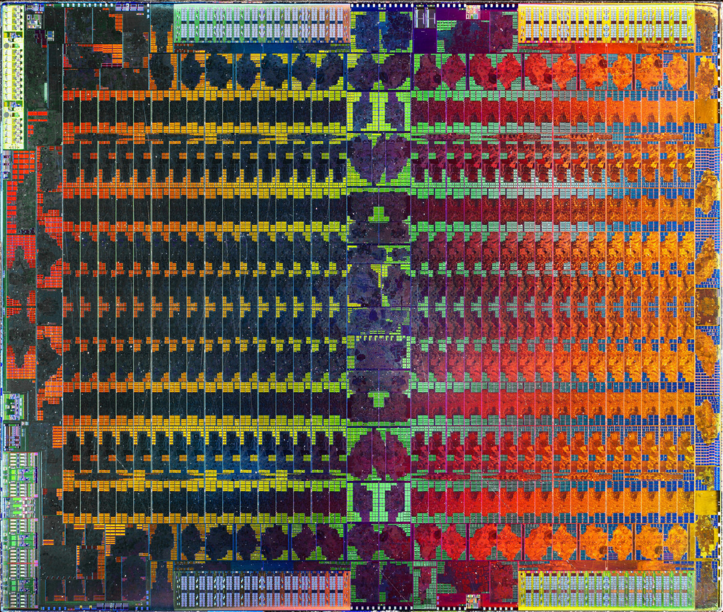
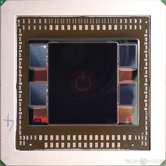
Die Shot

Block Diagram

Geometry Diagram
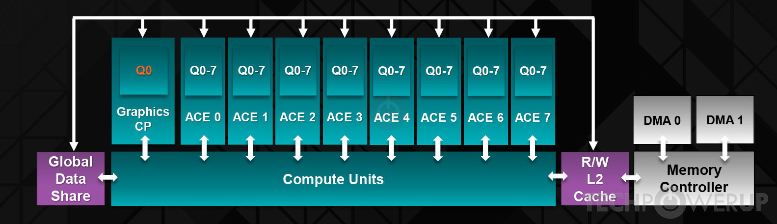
ACE Diagram
AMD's Capsaicin GPU uses the GCN 3.0 architecture and is made using a 28 nm production process at TSMC. With a die size of 596 mm² and a transistor count of 8,900 million it is a very big chip. Capsaicin supports DirectX 12 (Feature Level 12_0). For GPU compute applications, OpenCL version 2.1 can be used. It features 4096 shading units, 256 texture mapping units and 64 ROPs.
Further reading:
GCN 3.0 Instruction Set Architecture 
Graphics Processor
- Released
- Mar 31st, 2016
- GPU Name
- Capsaicin
- Desktop Variant
- Fiji
- Generation
- Pirate Islands
- Architecture
- GCN 3.0
- Foundry
- TSMC
- Process Size
- 28 nm
- Transistors
- 8,900 million
- Density
- 14.9M / mm²
- Die Size
- 596 mm²
Graphics Features
- DirectX
- 12 (12_0)
- OpenGL
- 4.6
- OpenCL
- 2.1
- Vulkan
- 1.2.170
- Shader Model
- 6.5
- WDDM
- 2.7
- Compute
- GFX8 (gfx803)
- DCE
- 10.0
- UVD
- 6.0
- VCE
- 3.0
- SDMA
- 3.0.0
- CLRX
- GCN 1.2.0
Render Config
- Shading Units
- 4096
- TMUs
- 256
- ROPs
- 64
- Compute Units
- 64
- Z-Stencil
- 256
- ACEs
- 8
- GEs
- 4
- L1 Cache
- 16 KB per CU
- L2 Cache
- 2048 KB
- Max. TDP
- 350 W
All GCN 3.0 GPUs
AMD GPU Architecture History
- 2024 RDNA 4.0
- 2024 RDNA 3.5
- 2023-2024 CDNA 3.0
- 2022-2024 RDNA 3.0
- 2021 CDNA 2.0
- 2020 CDNA 1.0
- 2020-2024 RDNA 2.0
- 2019-2020 RDNA 1.0
- 2018-2022 GCN 5.1
- 2017-2020 GCN 5.0
- 2016-2020 GCN 4.0
- 2014-2019 GCN 3.0
- 2013-2017 GCN 2.0
- 2011-2020 GCN 1.0
- 2010-2013 TeraScale 3
- 2009-2015 TeraScale 2
- 2005-2013 TeraScale
- 2005-2007 Ultra-Threaded SE
Graphics cards using the AMD Capsaicin GPU
| Name | Chip | Memory | Shaders | TMUs | ROPs | GPU Clock | Memory Clock |
|---|---|---|---|---|---|---|---|
| Capsaicin XT C9 | 4 GB | 4096 | 256 | 64 | 1050 MHz | 500 MHz | |
| Capsaicin XT C9 | 4 GB | 4096 | 256 | 64 | 1000 MHz | 500 MHz | |
| Capsaicin XT C1 | 4 GB | 4096 | 256 | 64 | 975 MHz | 500 MHz |


Capsaicin GPU Notes
| Generation: Pirate Islands Desktop Variant: Fiji Graphics/Compute: GFX8 (gfx803) Display Core Engine: 10.0 Unified Video Decoder: 6.0 Video Compression Engine: 3.0 System DMA: 3.0.0 CLRX: GCN 1.2.0 Latest Drivers: Windows 7: 64-bit: AMD Software: Adrenalin Edition 22.6.1 Windows 8.1: 64-bit: Radeon Software: Crimson ReLive Edition 17.4.4 / 17.7.1 Windows 10: 64-bit: AMD Software: Adrenalin Edition 22.6.1 |
Nov 18th, 2024 22:32 EST
change timezone
Latest GPU Drivers
New Forum Posts
- Black monitor screen.. only sometimes. (3)
- What Was Your First... (Gaming Related Things) (35)
- Post your Cinebench 2024 score (589)
- A Memorial to Kreij - Gone 9 years but never forgotten- check out the latest build(s) (3281)
- TPU's Nostalgic Hardware Club (19483)
- PC build decisions give me headaches- would you change? (3)
- P9X79 LE seems to have a short in the VRM (1)
- Anyone using a MSI MEG Z890 Ace? (5)
- New GameTech GPU benchmark. Share your results! (STEAM page live now) (150)
- NVIDIA App (35)
Popular Reviews
- AMD Ryzen 7 9800X3D Review - The Best Gaming Processor
- Quick Look: MOONDROP Quark2 Type-C In-Ear Monitors
- Valkyrie VK02 Lite Review
- Beelink GTi12 Ultra Mini-PC + EX Dock (Intel Core i9-12900H) Review
- NVIDIA App v1.0 Review
- Epomaker TH40 Wireless Mechanical Keyboard Review
- Redragon K1NG 8K Review
- Upcoming Hardware Launches 2024 (Updated Nov 2024)
- Quick Look: G.SKILL WigiDash PC Command Panel
- DDR5 Memory Performance Scaling with AMD Zen 5
Controversial News Posts
- AMD Falling Behind: Radeon dGPUs Absent from Steam's Top 20 (222)
- AMD Ryzen 7 9800X3D Stocks Vaporized in Retail, Being Scalped (151)
- AMD Introduces Next-Generation AMD Ryzen 7 9800X3D Processor, $479, Nov 7 (124)
- Apple and Samsung in the Fray to Acquire Intel: Rumor (123)
- AMD Ryzen 7 9800X3D Comes with 120W TDP, 5.20 GHz Boost, All Specs Leaked (120)
- Microsoft Offers $30 Windows 10 Security Extension for Home Users (118)
- AMD Ryzen 7 9800X3D Has the CCD on Top of the 3D V-cache Die, Not Under it (110)
- TechPowerUp is Hiring a Power Supply (PSU) Reviewer (105)