Report an Error

AMD Antigua

Antigua

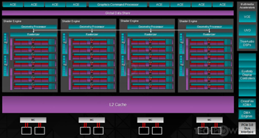
Block Diagram
AMD's Antigua GPU uses the GCN 3.0 architecture and is made using a 28 nm production process at TSMC. With a die size of 366 mm² and a transistor count of 5,000 million it is a large chip. Antigua supports DirectX 12 (Feature Level 12_0). For GPU compute applications, OpenCL version 2.1 can be used. It features 2048 shading units, 128 texture mapping units and 32 ROPs.
Further reading:
GCN 3.0 Instruction Set Architecture 
Graphics Processor
- Released
- May 5th, 2015
- GPU Name
- Antigua
- Desktop Variant
- Tonga
- Mobile Variant
- Amethyst
- Generation
- Volcanic Islands
- Architecture
- GCN 3.0
- Foundry
- TSMC
- Process Size
- 28 nm
- Transistors
- 5,000 million
- Density
- 13.7M / mm²
- Die Size
- 366 mm²
Graphics Features
- DirectX
- 12 (12_0)
- OpenGL
- 4.6
- OpenCL
- 2.1
- Vulkan
- 1.2.170
- Shader Model
- 6.5
- WDDM
- 2.7
- Compute
- GFX8 (gfx802)
- DCE
- 10.0
- UVD
- 5.0
- VCE
- 3.0
- SDMA
- 3.0.0
- CLRX
- GCN 1.2.0
Render Config
- Shading Units
- 2048
- TMUs
- 128
- ROPs
- 32
- Compute Units
- 32
- Z-Stencil
- 128
- ACEs
- 8
- GEs
- 4
- L1 Cache
- 16 KB per CU
- L2 Cache
- 512 KB
- Max. TDP
- 190 W
All GCN 3.0 GPUs
AMD GPU Architecture History
- 2023 CDNA 3.0
- 2022-2024 RDNA 3.0
- 2021 CDNA 2.0
- 2020 CDNA 1.0
- 2020-2023 RDNA 2.0
- 2019-2020 RDNA 1.0
- 2018-2022 GCN 5.1
- 2017-2020 GCN 5.0
- 2016-2020 GCN 4.0
- 2014-2019 GCN 3.0
- 2013-2017 GCN 2.0
- 2011-2020 GCN 1.0
- 2010-2013 TeraScale 3
- 2009-2015 TeraScale 2
- 2005-2013 TeraScale
- 2005-2007 Ultra-Threaded SE
Graphics cards using the AMD Antigua GPU
| Name | Chip | Memory | Shaders | TMUs | ROPs | GPU Clock | Memory Clock |
|---|---|---|---|---|---|---|---|
| Antigua PRO | 4 GB | 1792 | 112 | 32 | 918 MHz | 1375 MHz | |
| Antigua PRO | 2 GB | 1792 | 112 | 32 | 970 MHz | 1375 MHz | |
| Antigua XT | 4 GB | 2048 | 128 | 32 | 970 MHz | 1425 MHz |


Antigua GPU Notes
| Generation: Volcanic Islands Desktop Variant: Tonga Mobile Variant: Amethyst Graphics/Compute: GFX8 (gfx802) Display Core Engine: 10.0 Unified Video Decoder: 5.0 Video Compression Engine: 3.0 System DMA: 3.0.0 CLRX: GCN 1.2.0 |
May 21st, 2024 15:24 EDT
change timezone
Latest GPU Drivers
New Forum Posts
- Fractal define R4 vs R5 build quality. (23)
- EK seems to be having major issues (129)
- Kepler BIOS Tweaker problem (16)
- What is the best settings for i3 10100F? (2)
- Would a ag620 hold a 5700x3d in stock settings? (19)
- My anti budget PC (64)
- Post your cooling. (2)
- Ryzen 5 5600x stock overclocked reaching high temps (27)
- For general use - moving files around and playing games, would you have an Optane boot drive or PCie gen 5? (72)
- Gigabyte am5 motherboard ddr5 not posting when rebooting (8)
Popular Reviews
- Ghost of Tsushima Performance Benchmark Review - 35 GPUs Tested
- Ghost of Tsushima: DLSS vs. FSR vs. XeSS Comparison Review
- PNY XLR8 Gaming EPIC-X RGB DDR5-6400 CL32 32 GB Review
- TerraMaster D8 Hybrid Review
- Silverstone Shark Force 120 mm Fan Review
- Homeworld 3 Performance Benchmark Review - 35 GPUs Tested
- Upcoming Hardware Launches 2023 (Updated Feb 2024)
- Lofree Edge Ultra-Low Profile Wireless Mechanical Keyboard Review
- AMD Ryzen 7 7800X3D Review - The Best Gaming CPU
- AMD Ryzen 7 7700 Review - Affordable Zen 4 Powerhouse
Controversial News Posts
- Intel Statement on Stability Issues: "Motherboard Makers to Blame" (269)
- AMD to Redesign Ray Tracing Hardware on RDNA 4 (227)
- Windows 11 Now Officially Adware as Microsoft Embeds Ads in the Start Menu (173)
- NVIDIA to Only Launch the Flagship GeForce RTX 5090 in 2024, Rest of the Series in 2025 (154)
- AMD Hits Highest-Ever x86 CPU Market Share in Q1 2024 Across Desktop and Server (140)
- AMD RDNA 5 a "Clean Sheet" Graphics Architecture, RDNA 4 Merely Corrects a Bug Over RDNA 3 (139)
- AMD's RDNA 4 GPUs Could Stick with 18 Gbps GDDR6 Memory (114)
- AMD Ryzen 9 7900X3D Now at a Mouth-watering $329 (104)