Report an Error


AMD Seymour
Seymour

Seymour S3

Seymour PRO M2

Seymour XT M2

Seymour XTX M2

Block Diagram
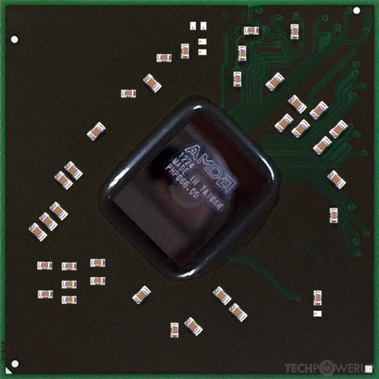
AMD's Seymour GPU uses the TeraScale 2 architecture and is made using a 40 nm production process at TSMC. With a die size of 67 mm² and a transistor count of 370 million it is a very small chip. Seymour supports DirectX 11.2 (Feature Level 11_0). For GPU compute applications, OpenCL version 1.2 can be used. It features 160 shading units, 8 texture mapping units and 4 ROPs.
Further reading:
TeraScale 2 Instruction Set Architecture 
Graphics Processor
- Released
- Oct 19th, 2010
- GPU Name
- Seymour
- Desktop Variant
- Caicos
- Generation
- Northern Islands
- Architecture
- TeraScale 2
- Foundry
- TSMC
- Process Size
- 40 nm
- Transistors
- 370 million
- Density
- 5.5M / mm²
- Die Size
- 67 mm²
- Package
- FCBGA-631/962
Graphics Features
- DirectX
- 11.2 (11_0)
- OpenGL
- 4.4
- OpenCL
- 1.2
- Vulkan
- N/A
- Shader Model
- 5.0
- WDDM
- 1.3
- Compute
- GFX4
- DCE
- 5.0
- UVD
- 3.1
Render Config
- Shading Units
- 160
- TMUs
- 8
- ROPs
- 4
- Compute Units
- 2
- Z-Stencil
- 16
- L1 Cache
- 8 KB per CU
- L2 Cache
- 128 KB
- Max. TDP
- 25 W
All TeraScale 2 GPUs
- AMD Barts
- AMD Blackcomb
- ATI Broadway
- AMD Broadway
- AMD Caicos
- AMD Capilano
- ATI Cedar
- AMD Cedar
- ATI Cypress
- AMD Cypress
- AMD Granville
- ATI Hemlock
- AMD Juniper
- ATI Juniper
- AMD Latte
- AMD Lexington
- AMD Loveland
- ATI Madison
- AMD Onega
- ATI Park
- AMD Park
- ATI Pinewood
- AMD Pinewood
- ATI Redwood
- AMD Redwood
- AMD Robson
- AMD Seymour
- AMD Sumo
- AMD SuperSumo
- AMD Thames
- AMD Turks
- ATI Turks
- AMD Whistler
AMD GPU Architecture History
Graphics cards using the AMD Seymour GPU
| Name | Chip | Memory | Shaders | TMUs | ROPs | GPU Clock | Memory Clock |
|---|---|---|---|---|---|---|---|
| Seymour XT M2 | 512 MB | 160 | 8 | 4 | 700 MHz | 800 MHz | |
| Seymour PRO S3 | 1024 MB | 160 | 8 | 4 | 600 MHz | 800 MHz | |
| Seymour LP S3 | 1024 MB | 160 | 8 | 4 | 480 MHz | 800 MHz | |
| Seymour XT M2 | 1024 MB | 160 | 8 | 4 | 750 MHz | 900 MHz | |
| Seymour XTX M2 | 1024 MB | 160 | 8 | 4 | 750 MHz | 900 MHz | |
| Seymour XTX M2 | 1024 MB | 160 | 8 | 4 | 800 MHz | 950 MHz | |
| Seymour XTX S3 | 512 MB | 160 | 8 | 4 | 800 MHz | 800 MHz | |
| Seymour PRO S3 | 1024 MB | 160 | 8 | 4 | 600 MHz | 800 MHz | |
| Seymour GL | 1024 MB | 160 | 8 | 4 | 750 MHz | 900 MHz | |
| Seymour XTX M2 | 256 MB | 160 | 8 | 4 | 750 MHz | 794 MHz | |
| Seymour LP S3 | 1024 MB | 160 | 8 | 4 | 480 MHz | 800 MHz |


Seymour GPU Notes
| Generation: Northern Islands Desktop Variant: Caicos Graphics/Compute: GFX4 Display Core Engine: 5.0 Unified Video Decoder: 3.1 |
Aug 14th, 2024 11:57 EDT
change timezone
Latest GPU Drivers
New Forum Posts
- AMD Ryzen 9 9900X Review (ign) (2)
- The Official Thermal Interface Material thread (1372)
- Have you got pie today? (16433)
- What Windows is overall the best to you and why? (139)
- Is alc 897/892 much worse than s1200a ? (3)
- AMD RX 7000 series GPU Owners' Club (1186)
- Buying board with some caps fallen off, worth it? (4)
- AM5 Build - I'm struggling a bit to land which motherboard and cpu to go with RX6800 (1)
- Improve thermal throttling - Surface Laptop Go 2 (6)
- VBIOS Flash changed the VRAM brand and now oc is unstable (6)
Popular Reviews
- We found the Missing Performance: Zen 5 Tested with SMT Disabled
- Cooler Master MasterBox 600 Review
- AMD Ryzen 7 9700X Review - The Magic of Zen 5
- AMD Ryzen 9 9950X Review - The New Flagship
- Razer Viper V3 Pro Review
- Endorfy Fluctus 120 PWM Fan Review
- AMD Ryzen 5 9600X Review - The Best Sub-$300 Gaming CPU
- ZMF BOKEH Closed-Back Dynamic Driver Headphones Review
- Kinesis Advantage360 Split Ergonomic Keyboard Review
- AMD Ryzen 9 9900X Review - But that Price
Controversial News Posts
- Intel Statement on 13th and 14th Gen Core Instability: Faulty Microcode Causes Excessive Voltages, Fix Out Soon (387)
- Intel Will Not Recall Failing 13th and 14th Gen CPUs (262)
- Several AMD RDNA 4 Architecture Ray Tracing Hardware Features Leaked (247)
- Faulty Windows Update from CrowdStrike Hits Banks and Airlines Around the World (234)
- Intel Stock Swandives 25% in Friday Trading Spooked by Quarterly Results (188)
- NVIDIA GeForce RTX 50 Series "Blackwell" TDPs Leaked, All Powered by 16-Pin Connector (167)
- AMD Delays Launch of Ryzen 9000 Series Processors (130)
- Intel Planning P-core Only "Bartlett" LGA1700 Processor for 2025 (127)