Report an Error


ATI R350
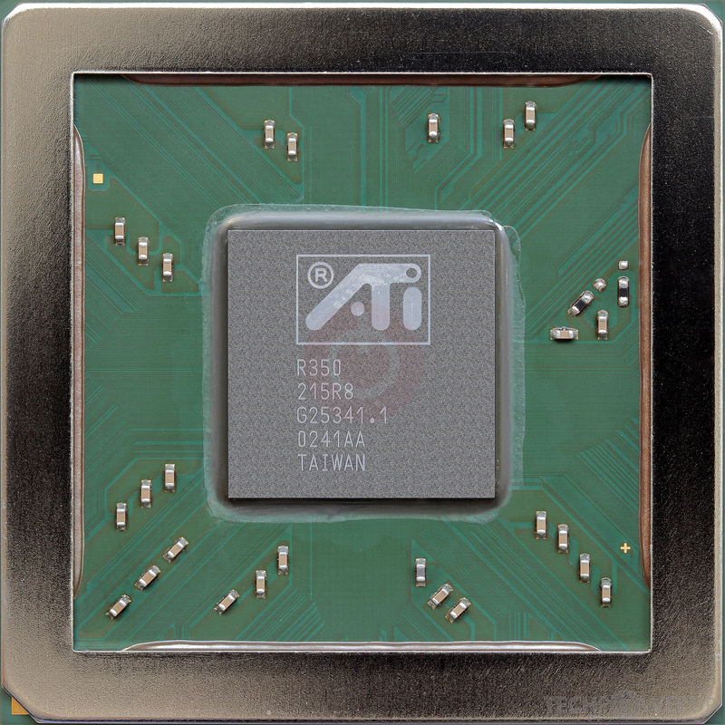
R350

R350 PRO

Die Shot
ATI's R350 GPU uses the R300 architecture and is made using a 150 nm production process at TSMC. With a die size of 215 mm² and a transistor count of 117 million it is a medium-sized chip. R350 supports DirectX 9.0 (Feature Level 9_0). Modern GPU compute technologies are not available. It features 8 pixel shaders and 4 vertex shaders, 8 texture mapping units and 8 ROPs. Due to the lack of unified shaders you will not be able to run recent games at all (which require unified shader/DX10+ support).
Graphics Processor
- Released
- Mar 1st, 2003
- GPU Name
- R350
- Codename
- Khan
- Architecture
- R300
- Foundry
- TSMC
- Process Size
- 150 nm
- Transistors
- 117 million
- Density
- 544.2K / mm²
- Die Size
- 215 mm²
Graphics Features
- DirectX
- 9.0 (9_0)
- OpenGL
- 2.0
- OpenCL
- N/A
- Vulkan
- N/A
- Pixel Shader
- 2.0
- Vertex Shader
- 2.0
- WDDM
- 1.0
- Compute
- GFX2
Render Config
- Pixel Shaders
- 8
- Vertex Shaders
- 4
- TMUs
- 8
- ROPs
- 8
- Max. TDP
- 94 W
All R300 GPUs
ATI GPU Architecture History
Graphics cards using the ATI R350 GPU
| Name | Chip | Memory | Shaders | TMUs | ROPs | GPU Clock | Memory Clock |
|---|---|---|---|---|---|---|---|
| R350 | 128 MB | 8 / 4 | 8 | 8 | 380 MHz | 340 MHz | |
| R350 SE | 128 MB | 4 / 4 | 4 | 4 | 378 MHz | 297 MHz | |
| R350 SE | 128 MB | 4 / 4 | 4 | 4 | 331 MHz | 290 MHz | |
| R350 | 128 MB | 8 / 4 | 8 | 8 | 378 MHz | 338 MHz | |
| R350 | 128 MB | 8 / 4 | 8 | 8 | 325 MHz | 290 MHz | |
| R350 | 128 MB | 8 / 4 | 8 | 8 | 380 MHz | 340 MHz | |
| R350 SE | 128 MB | 4 / 4 | 4 | 4 | 378 MHz | 297 MHz |


R350 GPU Notes
| Codename: Khan Graphics/Compute: GFX2 Smart Shader 2.1 Smooth Vision 2.1 TruForm 2.0 FullStream Hyper Z III+ Video Shader Video Immersion II Latest Drivers: Windows 98 / Me / 2000: Catalyst Software Suite 6.2 Windows XP / Vista: Catalyst Software Suite 10.2 |
Nov 20th, 2024 00:40 EST
change timezone
Latest GPU Drivers
New Forum Posts
- X299 Owners Club (86)
- Advise me before buying (98)
- 9800x 3d vs 12900k - Battle of the Century (129)
- Got an Asus X870E-E Strix board for the extra M.2 cooling & extra slot... issues abound. (33)
- Videocard MSI RX 580 ARMOR SP 8 GB (3)
- Is there a way to make web sites shut up about cookies? (26)
- Windows 11 24H2 is driving people to Linux (20)
- Technical Issues - TPU Main Site & Forum (2024) (392)
- Passmark Scores (55)
- Problem with the motherboard ProArt X870E stuck on the DRAM light (6)
Popular Reviews
- NVIDIA SFF-Ready System Build & Benchmark Review - Build Small, Play Big
- AMD Ryzen 7 9800X3D Review - The Best Gaming Processor
- Quick Look: Shanling M1 Plus Portable Audio Player
- Quick Look: MOONDROP Quark2 Type-C In-Ear Monitors
- Valkyrie VK02 Lite Review
- Upcoming Hardware Launches 2024 (Updated Nov 2024)
- NVIDIA App v1.0 Review
- Redragon K1NG 8K Review
- DDR5 Memory Performance Scaling with AMD Zen 5
- APNX V1-W Review
Controversial News Posts
- AMD Falling Behind: Radeon dGPUs Absent from Steam's Top 20 (222)
- AMD Ryzen 7 9800X3D Stocks Vaporized in Retail, Being Scalped (152)
- AMD Introduces Next-Generation AMD Ryzen 7 9800X3D Processor, $479, Nov 7 (124)
- Apple and Samsung in the Fray to Acquire Intel: Rumor (123)
- AMD Ryzen 7 9800X3D Comes with 120W TDP, 5.20 GHz Boost, All Specs Leaked (120)
- Microsoft Offers $30 Windows 10 Security Extension for Home Users (118)
- AMD Ryzen 7 9800X3D Has the CCD on Top of the 3D V-cache Die, Not Under it (110)
- TechPowerUp is Hiring a Power Supply (PSU) Reviewer (105)