Report an Error


ATI M22
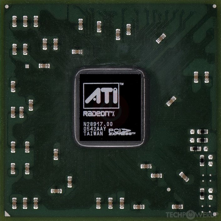
M22

M22 X300
ATI's M22 GPU uses the R300 architecture and is made using a 110 nm production process at TSMC. With a die size of 74 mm² and a transistor count of 107 million it is a very small chip. M22 supports DirectX 9.0b. Modern GPU compute technologies are not available. It features 4 pixel shaders and 2 vertex shaders, 4 texture mapping units and 4 ROPs. Due to the lack of unified shaders you will not be able to run recent games at all (which require unified shader/DX10+ support).
Graphics Processor
- Released
- Jun 1st, 2004
- GPU Name
- M22
- Desktop Variant
- RV370
- Codename
- Hari
- Architecture
- R300
- Foundry
- TSMC
- Process Size
- 110 nm
- Transistors
- 107 million
- Density
- 1.4M / mm²
- Die Size
- 74 mm²
Graphics Features
- DirectX
- 9.0b
- OpenGL
- 2.0
- OpenCL
- N/A
- Vulkan
- N/A
- Pixel Shader
- 2.0b
- Vertex Shader
- 2.0b
- WDDM
- 1.0
- Compute
- GFX2
Render Config
- Pixel Shaders
- 4
- Vertex Shaders
- 2
- TMUs
- 4
- ROPs
- 4
All R300 GPUs
ATI GPU Architecture History
Graphics cards using the ATI M22 GPU
| Name | Chip | Memory | Shaders | TMUs | ROPs | GPU Clock | Memory Clock |
|---|---|---|---|---|---|---|---|
| M22 X300 | 128 MB | 4 / 2 | 4 | 4 | 350 MHz | 250 MHz | |
| M22 GL | 128 MB | 4 / 2 | 4 | 4 | 350 MHz | 200 MHz |


M22 GPU Notes
| Desktop Variant: RV370 Codename: Hari Graphics/Compute: GFX2 Smart Shader 2.0 Smooth Vision 2.1 TruForm 2.0 FullStream Hyper Z III+ Video Shader Video Immersion II Programmable pixel&vertex pipelines |
Nov 20th, 2024 02:25 EST
change timezone
Latest GPU Drivers
New Forum Posts
- Glass mousepad (35)
- [INTEL]-How To Update Your Microcode for Intel HX 13/14th Gen. CPUs Laptops/Mobile Easily. (110)
- whats going on with core 2 quad and windows? (67)
- GPU-Z screenshots not working.. (1)
- Videocard MSI RX 580 ARMOR SP 8 GB (5)
- 9800x 3d vs 12900k - Battle of the Century (133)
- Crazy readings info with GPU-Z on Intel UHD Tiger GT1 (UHD) (4)
- Windows 11 24H2 is driving people to Linux (21)
- X299 Owners Club (86)
- Advise me before buying (98)
Popular Reviews
- NVIDIA SFF-Ready System Build & Benchmark Review - Build Small, Play Big
- AMD Ryzen 7 9800X3D Review - The Best Gaming Processor
- Quick Look: Shanling M1 Plus Portable Audio Player
- Quick Look: MOONDROP Quark2 Type-C In-Ear Monitors
- Valkyrie VK02 Lite Review
- Upcoming Hardware Launches 2024 (Updated Nov 2024)
- NVIDIA App v1.0 Review
- Redragon K1NG 8K Review
- APNX V1-W Review
- DDR5 Memory Performance Scaling with AMD Zen 5
Controversial News Posts
- AMD Falling Behind: Radeon dGPUs Absent from Steam's Top 20 (222)
- AMD Ryzen 7 9800X3D Stocks Vaporized in Retail, Being Scalped (152)
- AMD Introduces Next-Generation AMD Ryzen 7 9800X3D Processor, $479, Nov 7 (124)
- Apple and Samsung in the Fray to Acquire Intel: Rumor (123)
- AMD Ryzen 7 9800X3D Comes with 120W TDP, 5.20 GHz Boost, All Specs Leaked (120)
- Microsoft Offers $30 Windows 10 Security Extension for Home Users (118)
- AMD Ryzen 7 9800X3D Has the CCD on Top of the 3D V-cache Die, Not Under it (110)
- TechPowerUp is Hiring a Power Supply (PSU) Reviewer (105)