Report an Error


NVIDIA GeForce GTS 450 Rev. 2
- Graphics Processor
- GF116
- Cores
- 192
- TMUs
- 32
- ROPs
- 16
- Memory Size
- 1024 MB
- Memory Type
- GDDR5
- Bus Width
- 128 bit

GPU
Recommended Gaming Resolutions:
- 640x480
- 1280x720
- 1366x768
The GeForce GTS 450 Rev. 2 was a graphics card by NVIDIA, launched on March 15th, 2011. Built on the 40 nm process, and based on the GF116 graphics processor, in its GF116-200-KA-A1 variant, the card supports DirectX 12. Even though it supports DirectX 12, the feature level is only 11_0, which can be problematic with newer DirectX 12 titles. The GF116 graphics processor is an average sized chip with a die area of 238 mm² and 1,170 million transistors. It features 192 shading units, 32 texture mapping units, and 16 ROPs. NVIDIA has paired 1,024 MB GDDR5 memory with the GeForce GTS 450 Rev. 2, which are connected using a 128-bit memory interface. The GPU is operating at a frequency of 783 MHz, memory is running at 902 MHz (3.6 Gbps effective).
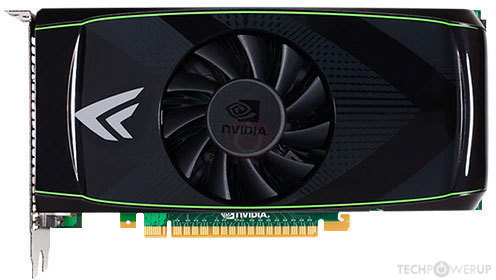
Being a dual-slot card, the NVIDIA GeForce GTS 450 Rev. 2 draws power from 1x 6-pin power connector, with power draw rated at 106 W maximum. Display outputs include: 2x DVI, 1x mini-HDMI 1.3a. GeForce GTS 450 Rev. 2 is connected to the rest of the system using a PCI-Express 2.0 x16 interface. The card measures 210 mm in length, and features a dual-slot cooling solution.
Being a dual-slot card, the NVIDIA GeForce GTS 450 Rev. 2 draws power from 1x 6-pin power connector, with power draw rated at 106 W maximum. Display outputs include: 2x DVI, 1x mini-HDMI 1.3a. GeForce GTS 450 Rev. 2 is connected to the rest of the system using a PCI-Express 2.0 x16 interface. The card measures 210 mm in length, and features a dual-slot cooling solution.
Graphics Processor
Graphics Card
- Release Date
- Mar 15th, 2011
- Generation
- GeForce 400
- Predecessor
- GeForce 200
- Successor
- GeForce 500
- Production
- End-of-life
- Bus Interface
- PCIe 2.0 x16
- Reviews
- 80 in our database
Relative Performance
Based on TPU review data: "Performance Summary" at 1920x1080, 4K for 2080 Ti and faster.
Performance estimated based on architecture, shader count and clocks.
Clock Speeds
- GPU Clock
- 783 MHz
- Shader Clock
- 1566 MHz
- Memory Clock
-
902 MHz
3.6 Gbps effective
Memory
- Memory Size
- 1024 MB
- Memory Type
- GDDR5
- Memory Bus
- 128 bit
- Bandwidth
- 57.73 GB/s
Render Config
- Shading Units
- 192
- TMUs
- 32
- ROPs
- 16
- SM Count
- 4
- L1 Cache
- 64 KB (per SM)
- L2 Cache
- 256 KB
Theoretical Performance
- Pixel Rate
- 6.264 GPixel/s
- Texture Rate
- 25.06 GTexel/s
- FP32 (float)
- 601.3 GFLOPS
- FP64 (double)
- 50.11 GFLOPS (1:12)
Board Design
- Slot Width
- Dual-slot
- Length
- 210 mm
8.3 inches
- TDP
- 106 W
- Suggested PSU
- 300 W
- Outputs
- 2x DVI
1x mini-HDMI 1.3a
- Power Connectors
- 1x 6-pin
- Board Number
- P1060 SKU 50,
P1062 SKU 1,
P1062 SKU 16,
P1428 SKU 10
Graphics Features
- DirectX
- 12 (11_0)
- OpenGL
- 4.6
- OpenCL
- 1.1
- Vulkan
- N/A
- CUDA
- 2.1
- Shader Model
- 5.1
GF116 GPU Notes
| PureVideo HD: VP4 VDPAU: Feature Set C Latest Drivers: Windows XP / Server 2003 x64: GeForce Release 368.81 Windows Vista: GeForce Release 365.19 Windows 7 / 8 / 8.1 / 10: GeForce Release 391.35 |
Retail boards based on this design (2)
| Name | GPU Clock | Memory Clock | Other Changes |
|---|---|---|---|
| 811 MHz | 902 MHz | 200 mm/7.9 inches, 1x DVI 1x HDMI 1x VGA | |
| 600 MHz | 666 MHz | 2 GB, DDR3, 170 mm/6.7 inches, Single-slot, 1x DVI 1x HDMI 1x DisplayPort |


Jul 12th, 2025 00:27 CDT
change timezone
Latest GPU Drivers
New Forum Posts
- Can you guess Which game it is? (220)
- What are you playing? (23920)
- RX 9070 XT freezing/locking up only on desktop, anyone else? (43)
- NVIDIA RTX PRO 6000 Workstation Runs Much Hotter Than 5090 FE (22)
- Quick charging your USB devicesUSB 3.2 Gen 2x2 Type-C® front-panel. (1)
- GTX 1050 GPU Owners Club (12)
- ASUS ProArt GeForce RTX 4060 Ti OC Edition 16GB GDDR6 Gaming - nvflash64 VBIOS mismatch (2)
- Will you buy a RTX 5090? (640)
- No offense, here are some things that bother me about your understanding of fans. (33)
- Best motherboards for XP gaming (102)
Popular Reviews
- Fractal Design Epoch RGB TG Review
- Corsair FRAME 5000D RS Review
- Lexar NM1090 Pro 4 TB Review
- NVIDIA GeForce RTX 5050 8 GB Review
- NZXT N9 X870E Review
- Sapphire Radeon RX 9060 XT Pulse OC 16 GB Review - An Excellent Choice
- AMD Ryzen 7 9800X3D Review - The Best Gaming Processor
- Upcoming Hardware Launches 2025 (Updated May 2025)
- Our Visit to the Hunter Super Computer
- Chieftec Iceberg 360 Review
TPU on YouTube
Controversial News Posts
- Intel's Core Ultra 7 265K and 265KF CPUs Dip Below $250 (288)
- Some Intel Nova Lake CPUs Rumored to Challenge AMD's 3D V-Cache in Desktop Gaming (140)
- AMD Radeon RX 9070 XT Gains 9% Performance at 1440p with Latest Driver, Beats RTX 5070 Ti (131)
- NVIDIA Launches GeForce RTX 5050 for Desktops and Laptops, Starts at $249 (119)
- NVIDIA GeForce RTX 5080 SUPER Could Feature 24 GB Memory, Increased Power Limits (115)
- Microsoft Partners with AMD for Next-gen Xbox Hardware (105)
- Intel "Nova Lake‑S" Series: Seven SKUs, Up to 52 Cores and 150 W TDP (100)
- NVIDIA DLSS Transformer Cuts VRAM Usage by 20% (97)