News Posts matching #18A

Return to Keyword Browsing

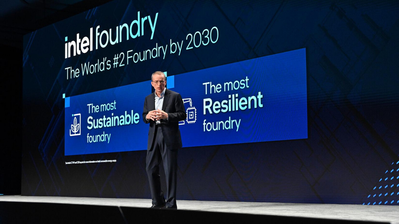
Intel Core Ultra 300 Series "Panther Lake-H" to Come with 64 W PL2 Power Configuration

Thanks to a well-known industry leaker, Jaykihn, Intel's Panther Lake-H processor family, built on the 18A process node, features three distinct configurations, with several power profiles for each case. The flagship model combines four "Cougar Cove" P-cores, eight "Skymont" E-cores, and four LPE cores alongside a 12-core Xe3 "Celestial" GPU. This variant supports LPDDR5X memory exclusively and delivers 180 TOPS of computational power for local AI workloads, operating at 25 W PL1 (base) and 64 W PL2 (turbo) power levels. Secondary configurations include a 4P+8E+4LP+4Xe3 model and a 4P+0E+4LP+4Xe3 variant, both rated at 100 TOPS and supporting both LPDDR5X and DDR5 memory.

The entry-level model operates at 15 W PL1 with 44 W PL2 in baseline mode, scaling to 25 W PL1 and 55 W PL2 in performance mode. All variants feature Thunderbolt 4 connectivity, with high-end models incorporating expanded PCIe 5.0 lane configurations. The integrated Xe3 graphics architecture scales from four to 12 cores across the product stack, with the top SKU eliminating DDR5 compatibility in favor of LPDDR5X optimization. The Panther Lake processor family is slated for launch within the latter half of 2025, and it will be the company's leading 18A product. As a "Lunar Lake" successor, Panther Lake will deliver improved IPC and optimization for new cores in the same device form-factor like laptops, ultrabooks, and handhelds.

Intel "Panther Lake" & "Wildcat Lake" SKU Details Leak Out

So far, this Friday (February 7) has been a bumper day for Intel CPU-related leaks. Golden Pig Upgrade and Jaykihn appear to be in competition with each other—they have uncovered all manner of speculative treasures across desktop and mobile segments. The latest revelation provides an early insight into unannounced feline-themed next-gen CPUs, courtesy of a Jaykihn social media post. Team Blue's Panther Lake processor family is slated for launch within the latter half of 2025—Intel officially stated that it would be their "lead product" on 18A. Older rumors had the "mobile-exclusive" Panther Lake processor family linked to a mixed configuration of new "Cougar Cove" P-cores and updated "Skymont" E-cores. According to today's leak, a variety of core configurations and feature sets are in the pipeline.

Jaykihn has listed three Panther Lake SKUs, and a "more mainstream" lower-end Wildcat Lake model. Common features include support for Thunderbolt 4 connectivity and LPDDR5X memory. Team Blue's rumored highest-end Panther Lake-H (PTL-H) processor appears to max out with a grand total of sixteen cores—consisting of 4 P-cores, 8 E-Cores, and 4 LP cores. The integrated graphics solution is (allegedly) a 12 core Xe3 "Celestial" GPU, with support for LPDDR5X memory—it is the only one on the list to completely jettison DDR5 compatibility. Insiders believe that the total platform (TOPS) rating is 180. As interpreted by VideoCardz, a 12-core "Panther Lake-U" (PTL-U) SKU is reportedly free of efficiency (E) units. The sole Wildcat Lake (WCL) model seems to sport a 2 P-core, 4-LP, and 2-Xe3 configuration.

Intel Pushes "Clearwater Forest" Xeon CPU Series Launch into 2026

Intel has officially announced that its "Clearwater Forest" Xeon processor family will be arriving somewhere in the first half of 2026. During a recent earnings call, interim co-CEO—Michelle Johnston Holthaus—discussed Team Blue's product roadmap for 2025 and beyond: "this year is all about improving Intel Xeon's competitive position as we fight harder to close the gap to the competition. The ramp of Granite Rapids has been a good first step. We are also making good progress on Clearwater Forest, our first Intel 18A server product that we plan to launch in the first half of next year." Press outlets have (correctly) pointed out that Intel's "Clearwater Forest" Xeon processors were originally slated for release in 2025, so the company's executive branch has seemingly admitted—in a low-key manner—that their next-gen series is delayed. Industry whispers from last autumn posit that Team Blue foundries were struggling with their proprietary 18A (1.8 nm) node process—at the time, watchdogs predicted a postponement of "Clearwater Forest" server processors.

The original timetable had "Clearwater Forest" server CPUs arriving not long after the launch of Intel's latest line of "Sierra Forest" products—288-core models from the Xeon 6-series. The delay into 2026 could be beneficial—The Register proposes that "Xeons bristling with E-cores" have not found a large enough audience. Holthaus disclosed a similar sentiment (in the Q4 earnings call): "what we've seen is that's more of a niche market, and we haven't seen volume materialize there as fast as we expected." Despite rumors swirling around complications affecting chip manufacturing volumes, Intel's temporary co-leaders believe that things are going well. David Zinsner—Team Blue's CFO—stated: "18A has been an area of good progress...Like any new process, there have been ups and downs along the way, but overall, we are confident that we are delivering a competitive process." His colleague added: "as the first volume customer of Intel 18A, I see the progress that Intel Foundry is making on performance and yield, and I look forward to being in production in the second half, as we demonstrate the benefits of our world-class design."

Speculative Intel "Nova Lake" CPU Core Configurations Leaked Online

Intel's freshly uploaded fourth-quarter 2024 "CEO/CFO earnings call comments" document has revealed grand CPU-related plans for 2025 and beyond. One of Team Blue's interim leaders—Michelle Johnston Holthaus—believes that "Nova Lake" processors (a next-generation client family) will arrive in 2026, following a comprehensive rollout of "Panther Lake" CPU products. This official timeline matches previously leaked and rumored development schedules—most notably, in a shipping manifest that was discovered last week. In recent times, industry watchdogs have linked "Nova Lake" to Intel's own 14A node and a TSMC 2 nm process node. Additionally, tipsters pointed to an apparent selection of Coyote Cove performance cores and Arctic Wolf efficiency-oriented cores.

Following yesterday's official announcements, a leaker shared several insights—theorized core configurations and manufacturing details were posted on the Hardware subreddit. Community members were engaged in a debate over Intel's "killing of Falcon Shore," but a plucky contributor—going under the moniker "Exist50"—redirected conversation to all-things "Nova Lake." They believe that Intel has shifted all "compute dies to TSMC" for manufacturing, after a change in plans—initial designs had the "8+16 die" on TSMC's N2P, and the "4+8 die on Intel 18A." Exist50 seemed to have inside track knowledge of product ranges: "Nova Lake (NVL) has a unified HUB/SoC die across mobile and desktop. So yeah, the baseline there is 4+8+4. But there's at least one more die for mobile." The flagship desktop (NVL-S or NVL-SK) chip's configuration could feature as many as sixteen performance cores and thirty-two efficiency cores, due to tile reuse—2x (8P+16E). Exist50 advised Intel CPU enthusiasts to forgo current generation offerings. "Nova Lake" should be: "quite a jump from Arrow Lake (ARL) in terms of MT performance, to say the least. I think anyone who buys ARL will end up regretting it, big time!"

Intel Confirms Panther Lake for 2H 2025, Nova Lake in 2026, Falcon Shores Canceled

Intel shared some news and updates about its upcoming CPU architectures during the Q4 earnings call. Intel confirmed that "Panther Lake", its next major CPU, is set to be released in late 2025. "Panther Lake" will use Intel's latest 18A manufacturing process and might be part of the Core Ultra 300 series. "Panther Lake" is rumored to combine next-generation "Cougar Cove" P-cores with existing "Skymont" E-cores both in the Compute complex, and in the SoC tile as low-power island E-cores. However, Intel hasn't confirmed if it will be available for desktop systems.

The following CPU architecture, "Nova Lake", is set to debut in 2026. Unlike "Panther Lake", we know "Nova Lake" will work on desktop computers. This suggests desktop users might need to wait until 2026 for an upgrade unless Intel surprises us with a desktop version of "Panther Lake" or an alternative option.

Intel "Nova Lake" Test CPU Appears, Targeting 2026 Launch

Shipping manifests at NBD.ltd have revealed the presence of Intel's "Nova Lake" test chips, providing insight into the development timeline of the company's 2026 processor platform. The discovery comes as Intel prepares for the launch of its "Panther Lake" CPUs on the 18A process node in late 2025. Nova Lake is positioned to replace both Panther Lake for mobile devices and "Arrow Lake" for desktop systems. The manufacturing process remains unconfirmed, with Intel potentially using either its in-house 14A node or TSMC's 2 nm technology. Following recent practices, Intel may split production between its own facilities and TSMC for different components. Rumored specifications show that Nova Lake will use Coyote Cove performance cores and Arctic Wolf efficiency cores.

Unlike Lunar Lake, it will not incorporate on-package memory, maintaining a more conventional design approach. The test chip's appearance suggests Intel is adhering to its development schedule. This timing aligns with the company's plans for Panther Lake's mass production in the second half of 2025, a structured transition between generations. Documents point to "Razor Lake" as Nova Lake's eventual successor, though detailed specifications are not yet available. Panther Lake, the immediate predecessor to Nova Lake, will focus primarily on mobile computing, with desktop variants limited to Mini PC implementations. This approach mirrors the Meteor Lake generation, which saw limited desktop release through the "PS" series for Edge platforms. The Nova Lake platform is expected to support DDR5 memory and may introduce PCIe Gen 6.0 compatibility, with final specifications unconfirmed.

Intel Foundry Adds New Customers to RAMP-C Project for US Defense

Intel Foundry has announced the onboarding of new defense industrial base (DIB) customers, Trusted Semiconductor Solutions and Reliable MicroSystems, as part of the third phase of the Rapid Assured Microelectronics Prototypes - Commercial (RAMP-C) efforts under the Trusted & Assured Microelectronics (T&AM) Program in the Office of the Under Secretary of Defense for Research and Engineering (OUSD (R&E)). The RAMP-C project, awarded through the Strategic & Spectrum Missions Advanced Resilient Trusted Systems (S²MARTS) Other Transaction Authority (OTA), allows DIB customers to take advantage of Intel Foundry's leading-edge Intel 18A process technology and advanced packaging for prototypes and high-volume manufacturing of commercial and DIB products for the U.S. Department of Defense (DoD).

"We are very excited to welcome Trusted Semiconductor Solutions and Reliable MicroSystems to the RAMP-C project we are engaged in with the DoD. The collaboration will drive cutting-edge, secure semiconductor solutions essential for our nation's security, economic growth and technological leadership. We are proud of the pivotal role Intel Foundry plays in supporting U.S. national defense and look forward to working closely with our newest DIB customers to enable their innovations with our leading-edge Intel 18A technology," said Kapil Wadhera, vice president of Intel Foundry and general manager of Aerospace, Defense and Government Business Group.

Intel "Panther Lake" Confirmed for 2025 Launch, Based on Intel 18A Node

Intel at its 2025 International CES keynote unveiled its next-generation mobile processor, codenamed "Panther Lake." Intel confirmed that the chip will be built on its homebrew Intel 18A foundry node. The current "Lunar Lake" and "Arrow Lake" processors see the company leverage TSMC N3 node for the Compute tiles. "Panther Lake" would see the x86-64 core IP return to an Intel node. "Panther Lake" is rumored to combine next-generation "Cougar Cove" P-cores with existing "Skymont" E-cores both in the Compute complex, and in the SoC tile as low-power island E-cores. "Panther Lake" is expected to debut in the second half of 2025.

Intel's "Wildcat Lake" Emerges as New Entry-Level Processor Series

According to recently discovered shipping manifests, Intel is developing a new processor series codenamed "Wildcat Lake," potentially succeeding their entry-level "Intel Processor" lineup based on Alder Lake-N. The documents, revealed by x86deadandback, suggest a 2025 launch timeline for these chips targeting lightweight laptops and mini-PCs. The shipping records from October 30 mention CPU reball equipment compatible with BGA 1516 sockets, measuring 35 x 25 mm, indicating early validation testing is underway. These processors are expected to be manufactured using Intel's advanced 18A process technology, sharing the same manufacturing node as the upcoming Panther Lake series. Early technical specifications of Wildcat Lake point to a hybrid architecture combining next-generation "Cougar Cove" performance cores with "Darkmont" low-power efficiency (LPE) cores in a 2P+4LPE configuration.

This design appears to separate the core clusters, departing from traditional shared ring bus arrangements, similar to the approach taken in Intel's Lunar Lake and Arrow Lake processors. While Wildcat Lake's exact position in Intel's product stack remains unclear, it could serve as a modernized replacement for the what were Pentium and Celeron processor families. These chips traditionally power devices like Chromebooks, embedded systems, and home servers, with the new series potentially offering significant performance improvements for these market segments. The processor is expected to operate in the sub-double-digit TDP power envelope, positioning it below the more powerful Lunar Lake series. Graphics capabilities will likely be more modest than Lunar Lake's Xe2 architecture, aligning with its entry-level market positioning.

Intel "Panther Lake" Confirmed on 18A Node, Powering-On With ES0 Silicon Revision

During Barclays 22nd Annual Global Technology Conference, Intel was a guest and two of the interim company co-CEOs Michelle Johnston Holthaus and David Zinsner gave a little update on the state of affairs at Intel. One of the most interesting aspects of the talk was Intel's upcoming "Panther Lake" processor—a direct successor to Intel Core Ultra 200S "Arrow Lake-H" mobile processors. The company confirmed that Panther Lake would utilize an Intel 18A node and that a few select customers have powered on Panther Lake on the E0 engineering sample chip. "Now we are using Intel Foundry for Panther Lake, which is our 2025 product, which will land on 18A. And this is the first time that we're customer zero in a long time on an Intel process," said interim co-CEO Michelle Johnston Holthaus, adding, "But just to give some assurances, on Panther Lake, we have our ES0 samples out with customers. We have eight customers that have powered on, which gives you just kind of an idea that the health of the silicon is good and the health of the Foundry is good."

While we don't know what ES0 means for Intel internally, we can assume that it is one of the first engineering samples on the 18A. The "ES" moniker usually refers to engineering samples, and zero after it could be the first design iteration. For reference, Intel's "Panther Lake-H" will reportedly have up to 18 cores: 6 P-cores, 8 E-cores, and 4 LP cores. The design brings back low-power island E-cores in the SoC tile. The P-cores use "Cougar Cove," which should have a higher IPC than "Lion Cove," while keeping the existing "Skymont" E-cores. The SoC tile may move from Arrow Lake's 6 nm to a newer process to fit the LP cores and an updated NPU. The iGPU is said to use the Xe3 "Celestial" architecture. With Arrow Lake-H launching in early 2025, Panther Lake-H likely won't arrive until 2026.

Intel 18A Yields Are Actually Okay, And The Math Checks Out

A few days ago, we published a report about Intel's 18A yields being at an abysmal 10%. This sparked quite a lot of discussion among the tech community, as well as responses from industry analysts and Intel's now ex-CEO Pat Gelsinger. Today, we are diving into known information about Intel's 18A node and checking out what the yields of possible products could be, using tools such as Die Yield Calculator from SemiAnalysis. First, we know that the defect rate of the 18A node is 0.4 defects per cm². This information is from August, and up-to-date defect rates could be much lower, especially since semiconductor nodes tend to evolve even when they are production-ready. To measure yields, manufacturers use various yield models based on the information they have, like the aforementioned 0.4 defect density. Expressed in defects per square centimeter (def/cm²), it measures manufacturing process quality by quantifying the average number of defects present in each unit area of a semiconductor wafer.

Measuring yields is a complex task. Manufacturers design some smaller chips for mobile and some bigger chips for HPC tasks. Thus, these two would have different yields, as bigger chips require more silicon area and are more prone to defects. Smaller mobile chips occupy less silicon area, and defects occurring on the wafer often yield more usable chips than wasted silicon. Stating that a node only yields x% of usable chips is only one side of the story, as the size of the test production chip is not known. For example, NVIDIA's H100 die is measuring at 814 mm²—a size that is pushing modern manufacturing to its limits. The size of a modern photomask, the actual pattern mask used in printing the design of a chip to silicon wafer, is only 858 mm² (26x33 mm). Thus, that is the limit before exceeding the mask and needing a redesign. At that size, nodes are yielding much less usable chips than something like a 100 mm² mobile chip, where defects don't wreak havoc on the yield curve.

Intel's Foundry Plan Remains the Same, Interim Co-CEO David Zinsner Confirms

Intel's Foundry business is the company's current pain point and probably the reason why the company board of directors forced out ex-CEO Pat Gelsinger. However, the new interim co-CEO, David Zinsner, confirmed that the foundry plan would remain the same. At the UBS technology conference, Zinsner indicated that the company's core strategy remains unchanged and reiterated the forecasts shared in October, highlighting optimism about growth in its PC and server segments. This is a healthy sign that Intel will not lose its foundry subsidiary, which, even though difficult to operate, could be Intel's silver lining with growth opportunities ahead.

Yesterday, we covered the choice of Lip-Bu Tan as Intel's next CEO. However, the new co-CEO, Zinsner, stated, "I'm not in the process, but I'm guessing that the CEO will have some capability around foundry as well as on the product side." A new CEO would be left with a lot of work that, apparently, no one so far can finish. There are speculations that Intel's 18A node is yielding 10% of usable silicon, while Intel's head of foundry business, Naga Chandrasekaran, has noted that 18A node is going through evolution phases to improve final yields and remain profitable, noting that "there's nothing fundamentally challenging on this node now. It is about going through the remaining yield challenges, defect density challenges."

Intel 18A Process Node Clocks an Abysmal 10% Yield: Report

In case you're wondering why Intel went with TSMC 3 nm to build the Compute tile of its "Arrow Lake" processor, and the SoC tile of "Lunar Lake," instead of Intel 3, or even Intel 20A, perhaps there's more to the recent story about Broadcom voicing its disappointment in the Intel 18A foundry node. The September 2024 report didn't specify a number to what yields on the Intel 18A node looked like to spook Broadcom, but we now have some idea as to just how bad things are. Korean publication Chosun, which tracks developments in the electronics and ICT industries, reports that yields on the Intel 18A foundry node stand at an abysmal 10%, making it unfit for mass-production. Broadcom validated Intel 18A as it was prospecting a cutting-edge node for its high-bandwidth network processors.

The report also hints that Intel's in-house foundry nodes going off the rails could be an important event leading up to the company's Board letting go of former CEO Pat Gelsinger, as huge 2nd order effects will be felt across the company's entire product stack in development. For example, company roadmaps put the company's next-generation "Clearwater Forest" server processor, slated for 2025, as being designed for the Intel 18A node. Unless Intel Foundry can pull a miracle, an effort must be underway to redesign the chip for whichever TSMC node is considered cutting-edge in 2025.

Intel's $7.86 Billion CHIPS Act Grant Forbids Selling Its Foundry Business

When Intel announced the completion of its $7.86 billion CHIPS Act grant from the Biden-Harris administration on Tuesday, we assumed some special terms were tied to the grant. Intel is essentially making a law-abiding promise to the US government that it will not sell its stake in the Intel Foundry unit under any circumstances, even if it manages to become an independent entity. This ensures that Intel is the major voting party in any event. Intel disclosed in a regulatory document that if Intel Foundry becomes its own private entity, Intel must maintain majority control with at least 50.1% ownership to keep its subsidy agreements. Additionally, if Intel Foundry goes public in the future, no single investor would be allowed to acquire more than 35% of shares unless Intel remains the largest shareholder, as this would trigger control-change clauses.

This essentially positions Intel Foundry as too big and too important of a unit to fail, both for Intel and the US government. Given Intel's ties with the US Department of Defense, with up to $3 billion in direct funding under the CHIPS and Science Act for the Secure Enclave program, Intel is vital for providing the US government with advanced semiconductor manufacturing. Strategically, Intel Foundry is the sole US-based company that competes with advanced manufacturing companies such as TSMC and Samsung. Even with TSMC and Samsung driving investments on US soil with advanced fabs, Intel's work with the government requires additional safety and secrecy clearances that only a US firm could provide. In the latest Q3 2024 financial results, Intel Foundry recorded a revenue of $4.4 billion with $5.8 billion in losses. While the operating marking of negative 134.3% seems like a disaster, upcoming quarters will bring it to a positive with more customers and using already developed nodes like 18A.

Intel Could Manufacture Apple's Next-Generation A20 SoC for iPhone

Apple is reportedly considering diversifying its chip manufacturing strategy with a new silicon manufacturer: Intel. While the upcoming iPhone 17 series, expected next year, will likely feature A19 chips produced by TSMC, a recent rumor from Chinese leaker Fixed Focus Digital hints at a potential switch to Intel for the A20 chipsets powering the 2026 iPhone 18 series. The A18 and A18 Pro chipsets debuted alongside the iPhone 16 series in September 2024, manufactured using TSMC's N3E node. Apple's A19 chips are expected to upgrade to TSMC's N3P node. According to the source, Apple is seeking an Intel 20A node. However, since the A20 node is canceled in favor of 18A, Apple could be an Intel Foundry customer for either 18A or 14A nodes.

Despite the buzz, skepticism persists. Intel has historically struggled with process node transitions and even outsourced production of its Arrow Lake CPUs to TSMC, raising questions about its readiness to deliver on Apple's demands. On the other hand, alternative reports suggest Apple might stick with TSMC's yet-unnamed 2 nm node for the A20, maintaining continuity in its supply chain. As the iPhone 18 series remains two years away, much can change. For now, we are left speculating whether this rumored collaboration with Intel represents a new chapter in Apple's chipset innovation or just a rumor with little substance. If the US government mandates more domestic production, chip designers could be looking at some of the more local manufacturing options, like Intel does on US soil. That could force Apple, NVIDIA, AMD, and Qualcomm to look into Intel's offerings.

"Jaguar Shores" is Intel's Successor to "Falcon Shores" Accelerator for AI and HPC

Intel has prepared "Jaguar Shores," its "next-next" generation AI and HPC accelerator, successor to its upcoming "Falcon Shores" GPU. Revealed during a technical workshop at the SC2024 conference, the chip was unveiled by Intel's Habana Labs division, albeit unintentionally. This announcement positions Jaguar Shores as the successor to Falcon Shores, which is scheduled to launch next year. While details about Jaguar Shores remain sparse, its designation suggests it could be a general-purpose GPU (GPGPU) aimed at both AI training, inferencing, and HPC tasks. Intel's strategy aligns with its push to incorporate advanced manufacturing nodes, such as the 18A process featuring RibbonFET and backside power delivery, which promise significant efficiency gains, so we can expect to see upcoming AI accelerators incorporating these technologies.

Intel's AI chip lineup has faced numerous challenges, including shifting plans for Falcon Shores, which has transitioned from a CPU-GPU hybrid to a standalone GPU, and cancellation of Ponte Vecchio. Despite financial constraints and job cuts, Intel has maintained its focus on developing cutting-edge AI solutions. "We continuously evaluate our roadmap to ensure it aligns with the evolving needs of our customers. While we don't have any new updates to share, we are committed to providing superior enterprise AI solutions across our CPU and accelerator/GPU portfolio." an Intel spokesperson stated. The announcement of Jaguar Shores shows Intel's determination to remain competitive. However, the company faces steep competition. NVIDIA and AMD continue to set benchmarks with performant designs, while Intel has struggled to capture a significant share of the AI training market. The company's Gaudi lineup ends with third generation, and Gaudi IP will get integrated into Falcon Shores.

Intel Reportedly Ramps "Arrow Lake" Orders at TSMC Amid Internal Foundry Struggles

According to Taiwanese media Commercial Times, Intel is significantly increasing its outsourcing of "Arrow Lake" CPU production to TSMC, a strategic move as it grapples with persistent issues in its own foundry division. This decision to outsource a substantial portion of Arrow Lake's production is a significant shift in Intel's strategy, showing the company's rising reliance on external partners to meet quality and performance demands. The Arrow Lake Core Ultra 200 series is Intel's first major outsourcing initiative, in which Intel gave its core IP to third-party foundries, more specifically for a 3 nm node at TSMC. However, it clearly indicates the performance gaps in Intel's own Intel Foundry and the high demand expectations for the new CPUs. Originally intended to use Intel 20A node, Intel shifted focus of 18A node for its products and upcoming foundry customers.

Intel's recent orders with TSMC extend to its upcoming Lunar Lake chips and next-generation Falcon Shores AI GPUs, both of which will use TSMC's 3 nm process. Although Intel's 18A node remains promising, the company relies on current products to sustain its revenue streams, making TSMC's support crucial in ensuring timely shipments. This increased outsourcing reflects Intel's need to maintain competitive performance in the short term. Once its Foundry division meets performance and capacity targets, Intel aims to bring more CPU manufacturing back in-house. However, if anything goes wrong, Intel could face challenges securing sufficient volume from TSMC, as the foundry has longstanding commitments with major clients like Apple, NVIDIA, Qualcomm, and AMD.

Intel's Silver Lining is $8.5 Billion CHIPS Act Funding, Possibly by the End of the Year

Intel's recent financial woes have brought the company into severe cost-cutting measures, including job cuts and project delays. However, a silver lining remains—Intel is reportedly in the final stages of securing $8.5 billion in direct funding from the US government under the CHIPS Act, delivered by the end of the year. The potential financing comes at a crucial time for Intel, which has been grappling with financial challenges. The company reported a $1.6 billion loss in the second quarter of 2024, leading to short-term setbacks. However, thanks to sources close to the Financial Times, we learn that Intel's funding target will represent the CHIPS Act's largest share, leading to a massive boost to US-based semiconductor manufacturing.

Looking ahead, the potential CHIPS Act funding could serve as a catalyst for Intel's resurgence, reassuring both investors and customers about the company's future. A key element of Intel's recovery strategy lies in the ramp-up of production for its advanced 18A node, which should become the primary revenue driver for its foundry unit. This advancement, coupled with the anticipated government backing, positions Intel to potentially capture market share from established players like TSMC and Samsung. The company has already secured high-profile customers such as Amazon and (allegedly) Broadcom, hinting at its growing appeal in the foundry space. Moreover, Intel's enhanced domestic manufacturing capabilities align well with potential US government mandates for companies like NVIDIA and Apple to produce processors locally, a consideration driven by escalating geopolitical tensions.

Intel Core Ultra 300 Series "Panther Lake-H" Leaks: 18 CPU Cores, 12 Xe3 GPU Cores, and up to 45 Watt TDP

Details have emerged about Intel's upcoming "Panther Lake" processors, set to be the third generation of Core Ultra mobile chips. Called the Core Ultra 300 series, these CPUs are expected to succeed "Lunar Lake". According to recent leaks, Panther Lake-H will be manufactured using Intel's cutting-edge 18A process node. The chips are said to feature a combination of Cougar Cove P-Cores, Skymont E-Cores, and Xe3 (Celestial) integrated graphics. This architecture builds upon Intel's hybrid core design, refining it for even better performance on mobile devices. The leaked information suggests a range of configurations for Panther Lake-H, the high-perfomance variant of the lineup. These include models with varying core counts and power envelopes, from efficient 25 W parts to more interesting 45 W options. Notably, some SKUs reportedly feature up to 18 cores in total, combining P-cores, E-cores, and LP E-cores in a five-tile package. This is an increase from previously believed 16 cores.

Intel 20A Node Cancelled for Foundry Customers, "Arrow Lake" Mainly Manufactured Externally

Intel has announced the cancellation of its 20A node for Foundry customers, as well as shifting majority of Arrow Lake production to external foundries. The tech giant will instead focus its resources on the more advanced 18A node while relying on external partners for Arrow Lake production, likely tapping TSMC or Samsung for their 2 nm nodes. The decision follows Intel's successful release of the 18A Process Design Kit (PDK) 1.0 in July, which garnered positive feedback from the ecosystem, according to the company. Intel reports that the 18A node is already operational, booting operating systems and yielding well, keeping the company on track for a 2025 launch. This early success has enabled Intel to reallocate engineering resources from 20A to 18A sooner than anticipated. As a result, the "Arrow Lake processor family will be built primarily using external partners and packaged by Intel Foundry".

The 20A node, while now cancelled for Arrow Lake, has played a crucial role in Intel's journey towards 18A. It served as a testbed for new techniques, materials, and transistor architectures essential for advancing Moore's Law. The 20A node successfully integrated both RibbonFET gate-all-around transistor architecture and PowerVia backside power delivery for the first time, providing valuable insights that directly informed the development of 18A. Intel's decision to focus on 18A is also driven by economic factors. With the current 18A defect density already at D0 <0.40, the company sees an opportunity to optimize its engineering investments by transitioning now. However, challenges remain, as evidenced by recent reports of Broadcom's disappointment in the 18A node. Despite these hurdles, Intel remains optimistic about the future of its foundry services and the potential of its advanced manufacturing processes. The coming months will be crucial as the company works to demonstrate the capabilities of its 18A node and secure more partners for its foundry business.

Broadcom's Testing of Intel 18A Node Signals Disappointment, Still Not Ready for High-Volume Production

According to a recent Reuters report, Intel's 18A node doesn't seem to be production-ready. As the sources indicate, Broadcom has been reportedly testing Intel's 18A node on its internal company designs, which include an extensive range of products from AI accelerators to networking switches. However, as Broadcom received the initial production run from Intel, the 18A node seems to be in a worse state than initially expected. After testing the wafers and powering them on, Broadcom reportedly concluded that the 18A process is not yet ready for high-volume production. With Broadcom's comments reflecting high-volume production, it signals that the 18A node is not producing a decent yield that would satisfy external customers.

While this is not a good sign of Intel's Fundry contract business development, it shows that the node is presumably in a good state in terms of power/performance. Intel's CEO Pat Gelsinger confirmed that 18A is now at 0.4 d0 defect density, and it is now a "healthy process." However, alternatives exist at TSMC, which proves to be a very challenging competitor to take on, as its N7 and N5 nodes had a defect density of 0.33 during development and 0.1 defect density during high-volume production. This leads to better yields and lower costs for the contracting party, resulting in higher profits. Ultimately, it is up to Intel to improve its production process further to satisfy customers. Gelsinger wants to see Intel Foundry as "manufacturing ready" by the end of the year, and we can see the first designs in 2025 reach volume production. There are still a few more months to improve the node, and we expect to see changes implemented by the end of the year.

Intel 18A Powers On, Panther Lake and Clearwater Forest Out of the Fab and Booting OS

Intel today announced that its lead products on Intel 18A, Panther Lake (AI PC client processor) and Clearwater Forest (server processor), are out of the fab and have powered-on and booted operating systems. These milestones were achieved less than two quarters after tape-out, with both products on track to start production in 2025. The company also announced that the first external customer is expected to tape out on Intel 18A in the first half of next year.

"We are pioneering multiple systems foundry technologies for the AI era and delivering a full stack of innovation that's essential to the next generation of products for Intel and our foundry customers. We are encouraged by our progress and are working closely with customers to bring Intel 18A to market in 2025." -Kevin O'Buckley, Intel senior vice president and general manager of Foundry Services

Intel's Panther Lake CPU Generation on Track for Mid-2025 Release, AI Capabilities to See Significant Boost

Intel's CEO, Pat Gelsinger, has confirmed that the upcoming 18A process of the Panther Lake CPU generation is on schedule for a mid-2025 release, which aligns with the initial projection. This development marks a significant milestone in the company's ongoing efforts to integrate AI capabilities into its processors. The mid-2025 release date is expected to follow the debut of Intel's Arrow Lake process in late 2024 or early 2025, a release that holds the promise of significant advancements in AI computing. During Intel's Q1 2024 Quarterly Results, Gelsinger expressed confidence in the company's AI capabilities, stating that the Core Ultra platform currently delivers leadership AI performance and that the next-generation platforms, Lunar Lake and Arrow Lake, will launch later this year, tripling AI performance. He also mentioned that the Panther Lake generation, set to release in 2025, will grow AI performance up to an additional 2x.

The Panther Lake generation represents the culmination of three generations of work in a short time and is expected to continue Intel's iterative approach. This transition is marked by a shift from a hybrid architecture, a combination of different types of processors, to a disaggregated die, where different components of the processor are separated, as AI computing becomes increasingly prominent. This strategic move is aimed at optimizing AI performance and flexibility. This marks the third generation of the Intel Core Ultra series, following Ultra 100 (Meteor Lake), Ultra 200 (Arrow Lake), and Lunar Lake (200V). Intel's release strategy mirrors the pattern set by the Hybrid Architecture, with Alder Lake debuting in 2021, followed by Raptor Lake in 2022, and a refreshed Raptor Lake released last year to bridge the gap until LGA 1851 was ready. However, Intel's roadmap has seen adjustments in the past, such as the initial promise of an Arrow Lake release before the end of 2024, which was later retracted. The mid-2025 release of Panther Lake aligns with rumors of Arrow Lake's late 2024 or early 2025 debut, suggesting that the 18A process CPU generation could debut several months after Arrow Lake.

Intel Lunar Lake Chiplet Arrangement Sees Fewer Tiles—Compute and SoC

Intel Core Ultra "Lunar Lake-MX" will be the company's bulwark against Apple's M-series Pro and Max chips, designed to power the next crop of performance ultraportables. The MX codename extension denotes MoP (memory-on-package), which sees stacked LPDDR5X memory chips share the package's fiberglass substrate with the chip, to conserve PCB footprint, and give Intel greater control over the right kind of memory speed, timings, and power-management features suited to its microarchitecture. This is essentially what Apple does with its M-series SoCs powering its MacBooks and iPad Pros. Igor's Lab scored the motherlode on the way Intel has restructured the various components across its chiplets, and the various I/O wired to the package.

When compared to "Meteor Lake," the "Lunar Lake" microarchitecture sees a small amount of "re-aggregation" of the various logic-heavy components of the processor. On "Meteor Lake," the CPU cores and the iGPU sat on separate tiles—Compute tile and Graphics tile, respectively, with a large SoC tile sitting between them, and a smaller I/O tile that serves as an extension of the SoC tile. All four tiles sat on top of a Foveros base tile, which is essentially an interposer—a silicon die that facilitates high-density microscopic wiring between the various tiles that are placed on top of it. With "Lunar Lake," there are only two tiles—the Compute tile, and the SoC tile.

Intel and Arm Team Up to Power Startups

Intel and Arm have signed a memorandum of understanding that finalizes the Emerging Business Initiative, their collaboration to support the startup community. The initiative builds on the April 2023 multi-generation agreement to enable chip designers to build low-power compute system-on-chips (SoCs) on the Intel 18A process. Together, the companies will provide essential intellectual property (IP) and manufacturing support, while also making financial assistance available, to foster innovation and growth for startups developing a range of devices and servers built on Arm-based SoCs and manufactured by Intel Foundry. The Emerging Business Initiative was announced last month at Intel Foundry Direct Connect in San Jose, California.

"Intel Foundry and Arm share the belief that for technology to benefit everyone, the building blocks of innovation must be available to anyone. Startups play a crucial role in bringing the great promise of transformations like AI to reality. The Emerging Business Initiative provides a path for new companies to leverage leading-edge Arm-based SoCs and Intel Foundry's global manufacturing capabilities to make their ideas real," said Stuart Pann, Intel senior vice president and general manager of Foundry Services.
Return to Keyword Browsing
Feb 16th, 2025 07:34 EST change timezone

Popular Reviews

Controversial News Posts