News Posts matching #2027

Return to Keyword Browsing

Fujitsu Previews Monaka: 144-Core Arm CPU Made with Chiplets

Fujitsu has previewed its next-generation Monaka processor, a 144-core powerhouse for data center. Satoshi Matsuoka of the RIKEN Center for Computational Science showcased the mechanical sample on social media platform X. The Monaka processor is developed in collaboration with Broadcom and employs an innovative 3.5D eXtreme Dimension System-in-Package architecture featuring four 36-core chiplets manufactured using TSMC's N2 process. These chiplets are stacked face-to-face with SRAM tiles through hybrid copper bonding, utilizing TSMC's N5 process for the cache layer. A distinguishing feature of the Monaka design is its approach to memory architecture. Rather than incorporating HBM, Fujitsu has opted for pure cache dies below compute logic in combination with DDR5 DRAM compatibility, potentially leveraging advanced modules like MR-DIMM and MCR-DIMM.

The processor's I/O die supports cutting-edge interfaces, including DDR5 memory, PCIe 6.0, and CXL 3.0 for seamless integration with modern data center infrastructure. Security in the design is taken care of with the implementation of Armv9-A's Confidential Computing Architecture for enhanced workload isolation. Fujitsu has set ambitious goals for the Monaka processor. The company aims to achieve twice the energy efficiency of current x86 processors by 2027 while maintaining air cooling capabilities. The processor aims to do AI and HPC with the Arm SVE 2 support, which enables vector lengths up to 2048 bits. Scheduled for release during Fujitsu's fiscal year 2027 (April 2026 to March 2027), the Monaka processor is shaping up as a competitor to AMD's EPYC and Intel's Xeon processors.

Samsung Plans 400-Layer V-NAND for 2026 and DRAM Technology Advancements by 2027

Samsung is currently mass-producing its 9th generation V-NAND flash memory chips with 286 layers unveiled this April. According to the Korean Economic Daily, the company targets V-NAND memory chips with at least 400 stacked layers by 2026. In 2013, Samsung became the first company to introduce V-NAND chips with vertically stacked memory cells to maximize capacity. However, stacking beyond 300 levels proved to be a real challenge with the memory chips getting frequently damaged. To address this problem, Samsung is reportedly developing an improved 10th-generation V-NAND that is going to use the Bonding Vertical (BV) NAND technology. The idea is to manufacture the storage and peripheral circuits on separate layers before bonding them vertically. This is a major shift from the current Co-Packaged (CoP) technology. Samsung stated that the new method will increase the density of bits per unit area by 1.6 times (60%), thus leading to increased data speeds.

Samsung's roadmap is truly ambitious, with plans to launch the 11th generation of NAND in 2027 with an estimated 50% improvement in I/O rates, followed by 1,000-layer NAND chips by 2030. Its competitor, SK hynix, is also working on 400-layer NAND aiming to have the technology ready for mass production by the end of 2025, as we previously mentioned in August. Samsung, the current HBM market leader with a 36.9% market share have also plans for its DRAM sector intending to introduce the sixth-generation 10 nm DRAM, or 1c DRAM by the first half of 2025. Then we can expect to see Samsung's seventh-generation 1d nm (still on 10 nm) in 2026, and by 2027 the company hopes to release its first generation sub-10 nm DRAM, or 0a DRAM memory that will use a Vertical Channel Transistor (VCT) 3D structure similar to what NAND flash utilizes.

Intel Completes Second ASML High-NA EUV Machine Installation

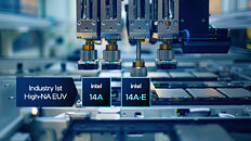
According to TechNews Taiwan, Intel has made significant progress in implementing ASML's cutting-edge High-NA EUV lithography technology. The company has successfully completed the assembly of its second High-NA "Twinscan EXE" EUV system at its Portland facility, as confirmed by Mark Phillips, Intel's Director of Lithography Hardware. Christophe Fouquet, CEO of ASML, highlighted that the new assembly process allows for direct installation at the customer's site, eliminating the need for disassembly and reassembly, thus saving time and resources. Phillips expressed enthusiasm about the technology, noting that the improvements offered by High-NA EUV machines have surpassed expectations compared to standard EUV systems. Given the massive $380 million price point of these High-NA systems, any savings are valuable in the process.

The rapid progress in installation and implementation of High-NA EUV technology at Intel's facilities positions the company strongly for production transition. With all necessary infrastructure in place and inspections of High-NA EUV masks already underway, Intel aims to have its Intel 14A process in mass production by 2026-2027. As Intel leads in High-NA EUV adoption, other industry giants are following suit. ASML plans to deliver High-NA EUV systems to TSMC by year-end, with rumors suggesting that TSMC's first system will possibly arrive in September. Samsung has also committed to the technology, although recent reports indicate a potential reduction in their procurement plans. Additionally, this development has sparked discussions about the future of photoresist technology, with Phillips suggesting that while Chemically Amplified Resist (CAR) is currently sufficient, future advancements may require metal oxide photoresists. This provides a small insight into Intel's future nodes.

TSMC's Next-Gen AI Packaging: 12 HBM4 and A16 Chiplets by 2027

During the Semicon Taiwan 2024 summit event, TSMC VP of Advanced Packaging Technology, Jun He, spoke about the importance of merging AI chip memory and logic chips using 3D IC technology. He predicted that by 2030 the worldwide semiconductor industry would hit the $1 trillion milestone with HPC and AI leading 40 percent of the market share. In 2027, TSMC will introduce the 2.5D CoWoS technology that includes eight A16 process chipsets and 12 HBM4. AI processors that use this technology will not only be much cheaper to produce but will also provide engineers with a greater level of convenience. Engineers will have the option to write new codes into them instead. Manufacturers are cutting the SoC and HBM architectural conversion and mass production costs down to nearly one-fourth.

Nevertheless, the increasing production capacities of 3D IC technology remain the main challenge, as the size of chips and the complexity of manufacturing are decisive factors. However, the higher the size of the chips, the more chiplets are added, and thus the performance is improved, but this now makes the process even more complicated and is associated with more risks of misalignment, breakage, and extraction failure.

Samsung to Install High-NA EUV Machines Ahead of TSMC in Q4 2024 or Q1 2025

Samsung Electronics is set to make a significant leap in semiconductor manufacturing technology with the introduction of its first High-NA 0.55 EUV lithography tool. The company plans to install the ASML Twinscan EXE:5000 system at its Hwaseong campus between Q4 2024 and Q1 2025, marking a crucial step in developing next-generation process technologies for logic and DRAM production. This move positions Samsung about a year behind Intel but ahead of rivals TSMC and SK Hynix in adopting High-NA EUV technology. The system is expected to be operational by mid-2025, primarily for research and development purposes. Samsung is not just focusing on the lithography equipment itself but is building a comprehensive ecosystem around High-NA EUV technology.

The company is collaborating with several key partners like Lasertec (developing inspection equipment for High-NA photomasks), JSR (working on advanced photoresists), Tokyo Electron (enhancing etching machines), and Synopsys (shifting to curvilinear patterns on photomasks for improved circuit precision). The High-NA EUV technology promises significant advancements in chip manufacturing. With an 8 nm resolution capability, it could make transistors about 1.7 times smaller and increase transistor density by nearly three times compared to current Low-NA EUV systems. However, the transition to High-NA EUV comes with challenges. The tools are more expensive, costing up to $380 million each, and have a smaller imaging field. Their larger size also requires chipmakers to reconsider fab layouts. Despite these hurdles, Samsung aims for commercial implementation of High-NA EUV by 2027.

0patch Offers Additional Windows 10 Security Updates, Extending Usage Until 2030

0patch plans to combat Microsoft's ending Windows 10 support by offering unofficial security updates for the 2015 operating system. Microsoft is ending Windows 10 security updates on October 14, 2025, after which the OS will stop receiving patches for vulnerabilities. The Redmond giant will provide you with an option to update your Windows 10 build, however, with a hefty fee slapped. Extended Security Updates (ESU) pricing structure follows a tiered model that doubles each year. From October 2025 to October 2026, the cost is $61 per device. The following year, from October 2026 to October 2027, the price increases to $122 per device. In the final year, spanning October 2027 to October 2028, the cost rises to $244 per device. For users planning to maintain Windows 10 until October 2028, the total expense over the three-year period would amount to $427 per device.

However, 0patch, a company focused on providing unofficial security updates for Windows OSes, will provide Windows 10 users with free and paid security updates post-end of service. Their system focuses on delivering targeted "micropatches" for critical vulnerabilities that emerge after Microsoft's official support ends. These micropatches are designed to be extremely precise and minimal, often consisting of just a few CPU instructions. A key feature of 0patch's approach is its non-invasive nature. The patches are applied directly to running processes in the computer's memory, leaving the original Microsoft files untouched. This method allows for rapid deployment of security fixes without requiring system reboots or interrupting user activities. The patching process is designed to be seamless and virtually unnoticeable to users. For instance, a user working on a document wouldn't experience any disruption while a micropatch is being applied. This approach is particularly beneficial for servers, where continuous uptime is crucial, as patches can be implemented without any downtime.

Micron Confirms US Fab Expansion Plan: Idaho and New York Fabs by 2026-2029

Micron has announced more precise timeframes for the commencement of operations at its two new memory facilities in the United States during its Q3 FY2024 results presentation. The company expects these fabs, located in Idaho and New York, to begin production between late 2026 and 2029. The Idaho fab, currently under construction near Boise, is slated to start operations between September 2026 and September 2027. Meanwhile, the New York facility is projected to come online in the calendar year 2028 or later, pending the completion of regulatory and permitting processes. These timelines align with Micron's original plans announced in 2022 despite recent spending optimizations. The company emphasizes that these investments are crucial to support supply growth in the latter half of this decade.

Micron's capital expenditure for FY2024 is set at approximately $8 billion, with a planned increase to around $12 billion in FY2025. This substantial rise in spending, targeting a mid-30s percentage of revenue, will support various technological advancements and facility expansions. A substantial portion of this increased investment - over $2 billion - will be dedicated to constructing the new fabs in Idaho and New York. Additional funds will support high-bandwidth memory assembly and testing, as well as the development of other fabrication and back-end facilities. Sanjay Mehrotra, Micron's CEO, underscored the importance of these investments, stating that the new capacity is essential to meet long-term demand and maintain the company's market position. He added that these expansions, combined with ongoing technology transitions in Asian facilities, will enable Micron to grow its memory bit supply in line with industry demand.

Kioxia Optimistic About Introducing 1000-Layer 3D NAND by 2027

Kioxia presented a technology roadmap at the IWM 2024 conference in Seoul, projecting the development of 1,000-layer 3D NAND by 2027. This ambitious goal is based on extrapolating past trends, which saw NAND layers increase from 24 in 2014 to 238 in 2022. Kioxia's plan involves not only increasing layer count but also shrinking cell size and increasing bit levels from TLC (3 bits per cell) to QLC (4 bits per cell), and possibly even to PLC (5 bits per cell).

However, these advancements come with significant technical challenges. Etching the vertical connecting holes (through-silicon vias or TSVs) are harder to achieve and can lead to higher channel resistance. Kioxia proposes solutions such as using single-crystalline silicon instead of polysilicon and switching from tungsten to molybdenum to reduce resistance. They also suggest moving to multi-lane wordlines to reduce the die area needed for electrical connectivity.

Micron DRAM Production Plant in Japan Faces Two-Year Delay to 2027

Last year, Micron unveiled plans to construct a cutting-edge DRAM factory in Hiroshima, Japan. However, the project has faced a significant two-year delay, pushing back the initial timeline for mass production of the company's most advanced memory products. Originally slated to begin mass production by the end of 2025, Micron now aims to have the new facility operational by 2027. The complexity of integrating extreme ultraviolet lithography (EUV) equipment, which enables the production of highly advanced chips, has contributed to the delay. The Hiroshima plant will produce next-generation 1-gamma DRAM and high-bandwidth memory (HBM) designed for generative AI applications. Micron expects the HBM market, currently dominated by rivals SK Hynix and Samsung, to experience rapid growth, with the company targeting a 25% market share by 2025.

The project is expected to cost between 600 and 800 billion Japanese yen ($3.8 to $5.1 billion), with Japan's government covering one-third of the cost. Micron has received a subsidy of up to 192 billion yen ($1.2 billion) for construction and equipment, as well as a subsidy to cover half of the necessary funding to produce HBM at the plant, amounting to 25 billion yen ($159 million). Despite the delay, the increased investment in the factory reflects Micron's commitment to advancing its memory technology and capitalizing on the growing demand for HBM. An indication of that is the fact that customers have pre-ordered 100% of the HBM capacity for 2024, not leaving a single HBM die unused.

Samsung Roadmaps UFS 5.0 Storage Standard, Predicts Commercialization by 2027

Mobile tech tipster, Revegnus, has highlighted an interesting Samsung presentation slide—according to machine translation, the company's electronics division is already responding to an anticipated growth of "client-side large language model" service development. This market trend will demand improved Universal Flash Storage (UFS) interface speeds—Samsung engineers are currently engaged in: "developing a new product that uses UFS 4.0 technology, but increases the number of channels from the current 2 to 4." The upcoming "more advanced" UFS 4.0 storage chips could be beefy enough to be utilized alongside next-gen mobile processors in 2025. For example; ARM is gearing up "Blackhawk," the Cortex-X4's successor—industry watchdogs reckon that the semiconductor firm's new core is designed to deliver "great Large Language Model (LLM) performance" on future smartphones. Samsung's roadmap outlines another major R&D goal, but this prospect is far off from finalization—their chart reveals an anticipated 2027 rollout. The slide's body of text included a brief teaser: "at the same time, we are also actively participating in discussions on the UFS 5.0 standard."

Intel Ohio Fab Opening Delayed to 2027/2028

Construction of Intel's New Albany, Ohio fabrication site started back in late 2022—since then, a series of setbacks have caused anticipated timelines to slip. Team Blue's original plans included a 2025 opening ceremony—last month, this was amended to late 2026 or early 2027. New equipment deliveries have been affected by extreme weather conditions—Intel appears to be shoring up its flood prevention systems at their Licking County location. Ohio's Department of Development received a progress report at the start of this month, authored by Team Blue staffers—revised figures indicate that Fabrication sites 1 and 2 are expected to reach operational status somewhere within "2027-2028."

Jim Evers (Intel's Ohio Site Manager) stated: "we are making great progress growing the Silicon Heartland. In addition to the approximately $1.5 billion investment in completed spends through 12/31/23 referenced in the report, Intel has an additional $3 billion in contractually committed spends underway, totaling $4.5 billion committed toward our Ohio One projects." Intel committed a hefty $20 billion greenfield investment into the two Ohio wafer fab sites, but the latest progress report indicates that just under a quarter of that budget has trickled out of company coffers (so far). Evers's statement continued: "this investment is growing every day as we work to establish a new manufacturing campus to build leading-edge semiconductor chips right here in Ohio." A Tom's Hardware report reminds us about Team Blue's New Albany project receiving "over $2 billion in incentives." Industry rumors posit that the US government is readying a multi-billion dollar grant for Intel's Arizona facility.

Apple Reportedly Developing 20.3-inch Foldable MacBook for 2027 Launch

According to renowned Apple analyst Ming-Chi Kuo, Apple is actively working on a foldable 20.3-inch MacBook, with mass production expected to begin in 2027. In a recent post on X/Twitter, Kuo stated that this foldable MacBook is currently Apple's only foldable product with a clear development schedule. Kuo's revelation comes amidst frequent inquiries about whether Apple plans to mass-produce a foldable iPhone or iPad in 2025 or 2026. His latest survey indicates that while Apple may explore these options, the foldable MacBook is the only device with a definitive timeline. This is not the first time rumors have circulated about a potential foldable MacBook from Apple. In 2022, display industry analyst Ross Young and Bloomberg's Mark Gurman both reported that Apple was interested in launching a foldable device with a screen size of around 20 inches.

Details about the foldable MacBook's design remain scarce, but it is expected to feature a single foldable OLED display that can be used in various configurations, such as a laptop mode with a virtual keyboard on the lower half of the screen or as a large tablet when fully unfolded. While competitors like Samsung, Motorola, and Huawei have already released foldable smartphones, Apple appears to be more cautious, focusing on perfecting the technology before bringing a product to market. As the foldable device market evolves, it will be interesting to see how Apple's unique take on the form factor fares. As Apple's first foldable product, it will be interesting to see what design choices are made and what hardware configuration will be present. But we are still relatively far away from the actual release of 2027.

TSMC to Open Kumamoto Fab 1 on February 24, Fab 2 to Begin Operations in 2027

Taiwan Semiconductor Manufacturing Company (TSMC) is set to open its new semiconductor fabrication plant in Kumamoto Prefecture, Japan, on February 24. This facility, known as Japan Advanced Semiconductor Manufacturing (JASM), represents a significant milestone for Japan's semiconductor industry. JASM spans 52 hectares and is designed to produce mature 40, 22/28, and 12/16 nm fabrication technologies in the Fab 1. The Fab 1 has an initial monthly capacity of 40,000 300 mm wafers, scalable to 50,000 wafers per month in the near term. However, TSMC is set to expand the Kumamoto facility with Fab 2, which will produce 7 nm and 6 nm nodes and is scheduled to begin operations at the end of the 2027 calendar year. The Japanese government is set to subsidize the Fab 2 expansion with around $5 billion in aid. Combining Fab 1 and Fab 2, the JASM Kumamoto facility could produce 100,000 300 mm wafers per month once the production of Fab 2 starts. According to market research firm TrendForce, JASM provides significant additional capacity for TSMC amid a global chip shortage. It also boosts Japan's domestic chipmaking capabilities, reducing reliance on imports.

JASM is the first brand-new foreign-operated fab built in Japan. The Japanese government provided grants and tax breaks to incentivize Kumamoto Fab 1 construction as part of a national strategy to re-shore more semiconductor production and is now doing it again with Fab 2. TSMC also received subsidies from customers like Sony, SSS, DENSO and Toyota. Dr. CC Wei, CEO of TSMC, stated that JASM will "shape Japan's semiconductor landscape over the next decade." TrendForce analysts echo this sentiment, noting that JASM's advanced nodes will enable cutting-edge chip designs from Japanese automotive and consumer electronics brands. The inauguration ceremony on February 24 will be attended by TSMC partners, customers, and government representatives. JASM is expected to ramp up production over the coming year. TSMC has other non-Taiwan investments, like the facility in construction in Phoenix, Arizona, which will start mass production of chips by the end of 2027 or early 2028. At that point, the global semiconductor capacity constraints will ease significantly.
TSCM JASM

IDC Forecasts Artificial Intelligence PCs to Account for Nearly 60% of All PC Shipments by 2027

A new forecast from International Data Corporation (IDC) shows shipments of artificial intelligence (AI) PCs - personal computers with specific system-on-a-chip (SoC) capabilities designed to run generative AI tasks locally - growing from nearly 50 million units in 2024 to more than 167 million in 2027. By the end of the forecast, IDC expects AI PCs will represent nearly 60% of all PC shipments worldwide.

"As we enter a new year, the hype around generative AI has reached a fever pitch, and the PC industry is running fast to capitalize on the expected benefits of bringing AI capabilities down from the cloud to the client," said Tom Mainelli, group vice president, Devices and Consumer Research. "Promises around enhanced user productivity via faster performance, plus lower inferencing costs, and the benefit of on-device privacy and security, have driven strong IT decision-maker interest in AI PCs. In 2024, we'll see AI PC shipments begin to ramp, and over the next few years, we expect the technology to move from niche to a majority."

IDC Forecasts Spending on GenAI Solutions Will Reach $143 Billion in 2027 with a Five-Year Compound Annual Growth Rate of 73.3%

A new forecast from International Data Corporation (IDC) shows that enterprises will invest nearly $16 billion worldwide on GenAI solutions in 2023. This spending, which includes GenAI software as well as related infrastructure hardware and IT/business services, is expected to reach $143 billion in 2027 with a compound annual growth rate (CAGR) of 73.3% over the 2023-2027 forecast period. This is more than twice the rate of growth in overall AI spending and almost 13 times greater than the CAGR for worldwide IT spending over the same period.

"Generative AI is more than a fleeting trend or mere hype. It is a transformative technology with far-reaching implications and business impact," says Ritu Jyoti, group vice president, Worldwide Artificial Intelligence and Automation market research and advisory services at IDC. "With ethical and responsible implementation, GenAI is poised to reshape industries, changing the way we work, play, and interact with the world."

Fujitsu Details Monaka: 150-core Armv9 CPU for AI and Data Center

Ever since the creation of A64FX for the Fugaku supercomputer, Fujitsu has been plotting the development of next-generation CPU design for accelerating AI and general-purpose HPC workloads in the data center. Codenamed Monaka, the CPU is the latest creation for TSMC's 2 nm semiconductor manufacturing node. Based on Armv9-A ISA, the CPU will feature up to 150 cores with Scalable Vector Extensions 2 (SVE2), so it can process a wide variety of vector data sets in parallel. Using a 3D chiplet design, the 150 cores will be split into different dies and placed alongside SRAM and I/O controller. The current width of the SVE2 implementation is unknown.

The CPU is designed to support DDR5 memory and PCIe 6.0 connection for attaching storage and other accelerators. To bring cache coherency among application-specific accelerators, CXL 3.0 is present as well. Interestingly, Monaka is planned to arrive in FY2027, which starts in 2026 on January 1st. The CPU will supposedly use air cooling, meaning the design aims for power efficiency. Additionally, it is essential to note that Monaka is not a processor that will power the post-Fugaku supercomputer. The post-Fugaku supercomputer will use post-Monaka design, likely iterating on the design principles that Monaka uses and refining them for the launch of the post-Fugaku supercomputer scheduled for 2030. Below are the slides from Fujitsu's presentation, in Japenese, which highlight the design goals of the CPU.

IDC Forecasts Worldwide Quantum Computing Market to Grow to $7.6 Billion in 2027

International Data Corporation (IDC) today published its second forecast for the worldwide quantum computing market, projecting customer spend for quantum computing to grow from $1.1 billion in 2022 to $7.6 billion in 2027. This represents a five-year compound annual growth rate (CAGR) of 48.1%. The forecast includes base quantum computing as a service as well as enabling and adjacent quantum computing as a service.

The new forecast is considerably lower than IDC's previous quantum computing forecast, which was published in 2021. In the interim, customer spend for quantum computing has been negatively impacted by several factors, including: slower than expected advances in quantum hardware development, which have delayed potential return on investment; the emergence of other technologies such as generative AI, which are expected to offer greater near-term value for end users; and an array of macroeconomic factors, such as higher interest and inflation rates and the prospect of an economic recession.

Report Suggests German Government Prepping $22 Billion Aid Package for Native Chip Production

According to a report published by Bloomberg, the German government has formed plans to create €20 billion ($22 billion) of investments to aid in the growth of local semiconductor manufacturing. The article proposes that the organization is racing to bolster the country's technology sector, and is attempting to secure essential supplies of components. Various geopolitical issues have complicated matters in recent times. Funding will be made available to German and international companies, from Germany's (now diversified) Climate and Transformation reserve, over the next four years. The finance ministry responded to Bloomberg's query, and stated: "The draft for the economic plan 2024 and the financial plan until 2027 for the Climate and Transformation Fund are currently being prepared...This process has not yet been completed." Germany's economy ministry did not provide a statement/response to Bloomberg's queries.

Around 75% of the fund is reportedly set aside for multinational semiconductor firms including Intel Corporation (USA) and Taiwan Semiconductor Manufacturing Company Limited (TSMC). Bloomberg believes that Team Blue is due an allocation of €10 billion for investments in its new production facility, located close to Magdeburg, Germany. The government is allegedly deep into talks with TSMC regarding the foundation of a proposed €10 billion production base in the Dresden area—the likes of BMW, Mercedes-Benz and Volkswagen AG would benefit greatly with quicker access to (localized) microcontrollers manufacturing facilities. The government could subsidize half of that total investment (€5 billion). Infineon is possibly in line to receive a €1 billion aid package, since it is building a new fab location in Dresden.

New EU Rule: Gaming Handhelds Required to Have Replaceable Batteries by 2027

Last week the European Union agreed on the provisional adoption of a new regulation that "strengthens sustainability rules for batteries and waste batteries. The regulation will regulate the entire life cycle of batteries - from production to reuse and recycling - and ensure that they are safe, sustainable and competitive." More specific terms include: "by 2027 portable batteries incorporated into appliances should be removable and replaceable by the end-user, leaving sufficient time for operators to adapt the design of their products to this requirement. This is an important provision for consumers." Although gaming handhelds are not referred to in specifics within the European Council's (very general) press material, Overkill (a site specializing in Steam Deck, Nintendo Switch and adjacent platforms) sought to investigate this matter further.

The publication was able to get in direct contact with an unnamed source at the European Union, who confirmed that: "the batteries of gaming handhelds are covered by the batteries and waste batteries regulation." The article proposes that future battery requirements will likely not affect current generation products—a Steam Deck successor and Nintendo's hypothetical Switch 2 are perhaps the prime candidates for internal design revisions according to EU legislation set for 2027. Overkill anticipates that portable gaming device manufacturers are going to question some of the new rules—similar to how smartphone makers have appealed against certain decisions. A compromise could be agreed upon, with slightly refashioned handhelds not conforming 100% to the new standards.

EU Approves New Regulation for Smartphone Batteries - Must be User-Replaceable by 2027

The European Parliament has greenlit new rules relating to battery technologies that are likely to cause headaches for smartphone manufacturers (in particular). The organization published their summary of this environmentally conscious and sustainable strategy on June 14: "Parliament approved new rules for the design (on Wednesday), production and waste management of all types of batteries (including non-replaceable types) sold in the EU. With 587 votes in favor, nine against and 20 abstentions, MEPs endorsed a deal reached with the Council to overhaul EU rules on batteries and waste batteries. The new law takes into account technological developments and future challenges in the sector and will cover the entire battery life cycle, from design to end-of-life."

The section for portable device batteries (for smartphones, tablets and cameras) outlines new consumer rights, with a demand for easily removable and replaceable (DIY) cells. Smartphone manufacturers including market leaders Apple and Samsung will have to go back to the drawing board and figure out ways to reformat how their batteries are mounted and connected internally. Plenty of devices have their units sealed behind protective layers, requiring specialist tools and varying levels of user expertise to access and remove in a safe manner. The European Council has more work to do following their starter announcement: "(We) will now have to formally endorse the text before its publication in the EU Official Journal shortly after and its entry into force." News outlets have interpreted that these provisional rulings will go into effect by early 2027, but they also anticipate that big time players could appeal for extensions beyond that window.
Return to Keyword Browsing
Dec 21st, 2024 11:54 EST change timezone

New Forum Posts

Popular Reviews

Controversial News Posts