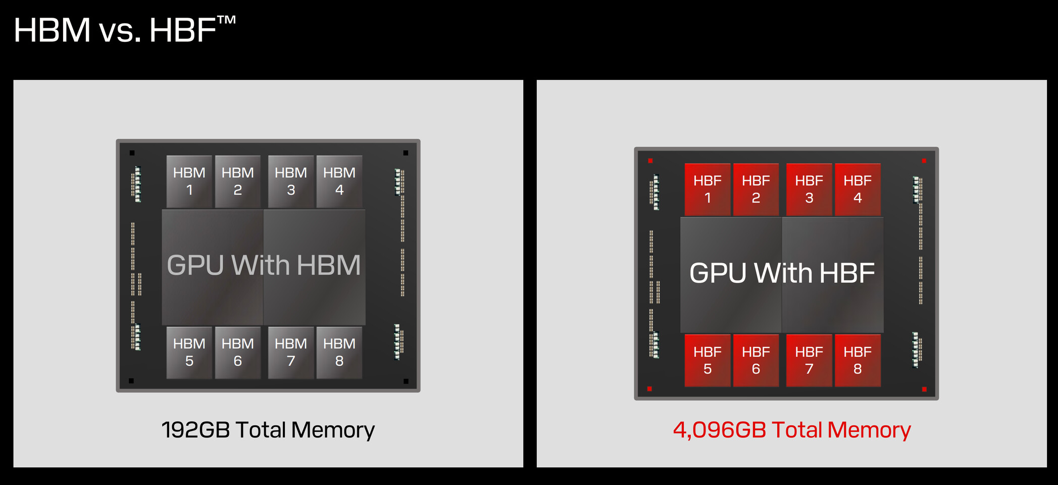
News Posts matching #3D NAND

Return to Keyword Browsing

NEO Semiconductor Announces 3D X-AI Chip as HBM Successor

NEO Semiconductor, a leading developer of innovative technologies for 3D NAND flash memory and 3D DRAM, announced today the development of its 3D X-AI chip technology, targeted to replace the current DRAM chips inside high bandwidth memory (HBM) to solve data bus bottlenecks by enabling AI processing in 3D DRAM. 3D X-AI can reduce the huge amount of data transferred between HBM and GPUs during AI workloads. NEO's innovation is set to revolutionize the performance, power consumption, and cost of AI Chips for AI applications like generative AI.

AI Chips with NEO's 3D X-AI technology can achieve:
  • 100X Performance Acceleration: contains 8,000 neuron circuits to perform AI processing in 3D memory.
  • 99% Power Reduction: minimizes the requirement of transferring data to the GPU for calculation, reducing power consumption and heat generation by the data bus.
  • 8X Memory Density: contains 300 memory layers, allowing HBM to store larger AI models.

Kingston Quietly Adds the NV3 to its SSD Lineup

Kingston's NV2 NVMe SSD has been a popular budget choice that has offered some of the best price/performance ratio in its segment of the market. Now, Kingston has quietly added its replacement, the NV3 to its website and that entails a wide range of upgrades over the NV2. The Kingston NV2 came in a range of different variations with multiple different controllers and NAND types and so far the company hasn't revealed which controller or what NAND the NV3 will feature. However, the company lists 3D NAND with a sequential read speeds of 6,000 MB/s for the 1 TB and up SKUs which is a huge improvement over the NV2 which topped out at 3,500 MB/s. Write speeds top out at 5,000 MB/s, but this is limited to the 2 and 4 TB SKUs, but it's nearly twice that of the 2 TB NV2 SKU. The 1 TB SKU is also seeing almost a doubling in terms of write speeds over the NV2. The 500 GB SKU is seeing more modest performance improvements, but it's still getting a decent performance uplift.

Initially, Kingston will launch 500 GB, 1 TB and 2 TB SKUs, with the 4 TB SKU following in Q4 this year. Endurance remains the same as for the NV2, with the NV3 starting out at 160 TBW for the 500 GB SKU, which then doubles for each increase in size and tops out at 1280 TBW for the 4 TB SKU. Kingston has as yet to officially announce the drive, but some online retailers claim to be able to ship the NV3 in four to five days time, suggesting that the launch is imminent. Pricing appears to start at US$50 for the 500 GB SKU, which increases to US$70 for the 1 TB SKU, with the 2 TB SKU jumping to US$139 from the same retailer. This places the NV3 slightly higher than the current retail price of the NV2, which is hardly a surprise, considering it delivers better performance. All SKUs come with a three year warranty.

SK hynix Targets 400-Layer NAND Production in 2025

SK hynix is reportedly developing 400-layer NAND flash memory, with plans to begin mass production by late 2025. The company is collaborating with supply chain partners to develop the necessary process technologies and equipment for 400-layer and higher NAND chips. This information comes from a recent article by Korean media outlet etnews citing industry sources.

SK hynix intends to use hybrid bonding technology to achieve this, which is expected to bring new packaging materials and components suppliers into the supply chain. The development process involves exploring new bonding materials and various technologies for connecting different wafers, including polishing, etching, deposition, and wiring. SK hynix aims to have the technology and infrastructure ready by the end of next year.

Lam Research Introduces Lam Cryo 3.0 Cryogenic Etch Technology to Accelerate Scaling of 3D NAND

Lam Research Corp. today extended its leadership in 3D NAND flash memory etching with the introduction of Lam Cryo 3.0, the third generation of the company's production-proven cryogenic dielectric etch technology. As the proliferation of generative artificial intelligence (AI) continues to propel the demand for memory with higher capacity and performance, Lam Cryo 3.0 provides etch capabilities critical for the manufacturing of future leading-edge 3D NAND. Leveraging ultra cold temperatures, high power confined plasma reactor technology, and innovations in surface chemistry, Lam Cryo 3.0 etches with industry-leading precision and profile control.

"Lam Cryo 3.0 paves the way for customers on the path to 1,000-layer 3D NAND," said Sesha Varadarajan, senior vice president of Global Products Group at Lam Research. "With five million wafers already manufactured using Lam cryogenic etch, our newest technology is a breakthrough in 3D NAND production. It creates high aspect ratio (HAR) features with angstrom-level precision, while delivering lower environmental impact and more than double the etch rate of conventional dielectric processes. Lam Cryo 3.0 is the etch technology our customers need to overcome the AI era's key NAND manufacturing hurdles."

Chinese Memory Manufacturer YMTC Sues Micron Over 3D NAND Patents

Chinese memory manufacturer YMTC has filed a lawsuit against U.S.-based Micron in California, alleging infringement of 11 patents related to 3D NAND Flash and DRAM products. YMTC seeks to halt Micron's sales of the allegedly infringing products in the U.S. and demands royalty payments. Founded in Wuhan, China, in 2016, YMTC is a key player in China's efforts to develop a domestic chip industry. However, in October 2022, the U.S. government placed YMTC on its Entity List, restricting its access to advanced U.S. manufacturing equipment for 3D NAND chips with 128 layers or more.

Before these restrictions, YMTC had obtained certification from Apple for its 128-layer 3D NAND chips, with the US tech giant considering using YMTC chips to reduce costs and diversify its supply chain beyond Samsung, SK Hynix and Micron. The lawsuit specifically targets Micron's 3D NAND Flash products with 96, 128, 176, and 232 layers, as well as certain DDR5 SDRAM products. This legal action follows a similar suit filed by YMTC against Micron in November, alleging infringement of eight U.S. patents related to 3D NAND Flash. With government backing, Chinese firms are increasingly engaging in patent litigation both domestically and internationally. Last year alone, Chinese courts handled over 5,000 technical intellectual property and monopoly cases.

Samsung Introduces 61.44 TB BM1743 SSD with 176-Layer V-NAND

Samsung has introduced its latest BM1743 SSD, boasting an impressive 61.44 TB of storage capacity. The BM1743 utilizes Samsung's seventh-generation 3D NAND (V-NAND) technology, featuring 176 layers of memory cells. This represents a significant leap from its predecessor, the BM1733, which debuted in 2020 with 96-layer technology and a maximum capacity of 32 TB. Performance-wise, the BM1743 doesn't disappoint. It delivers up to 1.6 million random read IOPS and 110,000 random write IOPS, with sequential read and write speeds of 7.2 GB/s and 2.0 GB/s, respectively. These figures position the drive as a highly capable solution for read-intensive workloads. Samsung claims that the new SSD offers double the sequential read and write speeds of its fifth-generation technology, with random reads quadrupling in performance. This advancement suggests that quad-level cell (QLC) SSDs are now approaching the performance levels of their triple-level cell (TLC) counterparts while offering superior storage density.

The BM1743 is available in the traditional U.2 form factor, with an E3.S variant supporting PCIe Gen 5 also in the lineup, thanks to the custom Samsung controller. Samsung has enhanced the durability and data retention capabilities of the BM1743. The new drive boasts an improved endurance rating of 0.26 drive writes per day (DWPD) throughout its warranty period, a notable increase from the BM1733's 0.18 DWPD. Additionally, the BM1743 extends its power-off data retention to three months, tripling the one-month period of its predecessor. In a hint of things to come, Samsung has suggested that a 122.88 TB model may be on the horizon, potentially doubling the capacity of the BM1743. This new offering puts Samsung in direct competition with Solidigm's D5-P5336, which has dominated the high-capacity SSD market for the past year. High-density storage solutions are becoming more important as AI and HPC tasks require and produce massive amounts of data.

Kioxia Optimistic About Introducing 1000-Layer 3D NAND by 2027

Kioxia presented a technology roadmap at the IWM 2024 conference in Seoul, projecting the development of 1,000-layer 3D NAND by 2027. This ambitious goal is based on extrapolating past trends, which saw NAND layers increase from 24 in 2014 to 238 in 2022. Kioxia's plan involves not only increasing layer count but also shrinking cell size and increasing bit levels from TLC (3 bits per cell) to QLC (4 bits per cell), and possibly even to PLC (5 bits per cell).

However, these advancements come with significant technical challenges. Etching the vertical connecting holes (through-silicon vias or TSVs) are harder to achieve and can lead to higher channel resistance. Kioxia proposes solutions such as using single-crystalline silicon instead of polysilicon and switching from tungsten to molybdenum to reduce resistance. They also suggest moving to multi-lane wordlines to reduce the die area needed for electrical connectivity.

Gigabyte Promises 219,000 TBW for New AI TOP 100E SSD

Gigabyte has quietly added a new SSD to its growing lineup and this time around it's something quite different. The drive is part of Gigabyte's new AI TOP (Trillions of Operations per Second) and was announced at Computex with little fanfare. At the show, the company only announced that it would have 150x the TBW compared to regular SSDs and that it was built specifically for AI model training. What that 150x means in reality is that the 2 TB version of the AI TOP 100E SSD will deliver no less than 219,000 TBW (TeraBytes Written), whereas most high-end 2 TB consumer NVMe SSDs end up somewhere around 1,200 TBW. The 1 TB version promises 109,500 TBW and both drives have an MTBF time of 1.6 million hours and a five-year warranty.

Gigabyte didn't reveal the host controller or the exact NAND used, but the drives are said to use 3D NAND flash and both drives have a LPDDR4 DRAM cache of 1 or 2 GB depending on the drive size. However, the pictures of the drive suggest it might be a Phison based reference design. The AI TOP 100E SSDs are standard PCIe 4.0 drives, so the sequential read speed tops out at 7,200 MB/s with the write speed for the 1 TB SKU being up to 6,500 MB/s, with the 2 TB SKU slightly behind at 5,900 MB/s. No other performance figures were provided. The drives are said to draw up to 11 Watts in use, which seems very high for PCIe 4.0 drives. No word on pricing or availability as yet.

NEO Semiconductor Reveals a Performance Boosting Floating Body Cell Mechanism for 3D X-DRAM during IEEE IMW 2024 in Seoul

NEO Semiconductor, a leading developer of innovative technologies for 3D NAND flash and DRAM memory, today announced a performance boosting Floating Body Cell Mechanism for 3D X-DRAM. Andy Hsu, Founder & CEO presented groundbreaking Technology CAD (TCAD) simulation results for NEO's 3D X-DRAM during the 16th IEEE International Memory Workshop (IMW) 2024 in Seoul, Republic of Korea.

Neo Semiconductor reveals a unique performance boosting mechanism called Back-gate Channel-depth Modulation (BCM) for Floating Body Cell that can increase data retention by 40,000X and sensing window by 20X.

Samsung Readies 290-layer 3D NAND for May 2024 Debut, Planning 430-layer for 2025

Samsung is preparing to launch its 9th Generation V-NAND (3D NAND flash) memory next month, Korean publication Hankyung reports. The 9th Gen 3D NAND flash memory by Samsung is expected to offer 290 layers, a step-up from the 236-layer 8th Gen V-NAND that the company debuted in 2022. Samsung reportedly achieved the 290-layer vertical stacking density through improvements in its flash layer stacking techniques that relies on increasing the layer counts through more memory holes in the flash layer. The cost here is data density per wafer, but a net gain from the increase in layer counts.

The same source behind the 9th Gen V-NAND story also reports that the company is targeting a rather early 2025 launch for its successor—the 10th Gen V-NAND. This is expected to be a mammoth 430-layer 3D NAND flash, a jump of 140 layers over the 9th Gen (which itself jumped by 54 layers over its predecessor). This would put Samsung back on track along with its competitors, Kioxia, SK Hynix, Micron Technology, and YMTC, as they gun for the ambitious goal of 1000-layer 3D NAND flash by 2030.
Many Thanks to TumbleGeorge for the tip.

MSI Announces the SPATIUM M580 FROZR: A Groundbreaking PCIe Gen 5 SSD Redefining Speed and Reliability

MSI, a global leader in gaming PC hardware, is thrilled to announce the release of its highly anticipated SSD powerhouse, the SPATIUM M580 FROZR, ushering in a new era of storage performance. With cutting-edge technology and innovative thermal solutions, this SSD is set to redefine the standards of speed and reliability in storage solutions.

SPATIUM M580 FROZR, Reaching New Heights with Crowned Speeds
The SPATIUM M580 FROZR sets a new benchmark in storage performance with its revolutionary features. Powered by the state-of-the-art PHISON E26 PCIe Gen 5 controller and equipped with advanced 3D NAND flash modules boasting 232 layers, this SSD achieves mind-blowing read speeds of up to 14.6 GB/s and write speeds of up to 12.7 GB/s, up to 2 times faster transfer rates compared to current PCIe 4.0 SSDs. This represents a significant leap in speeds, boosted by a DRAM cache buffer and a SLC Cache, providing users with lightning-fast data access and gaining valuable milliseconds in latency for gaming, content creation, and professional applications. Additionally, the M580 FROZR is fortified with LPDC ECC and E2E Data Protection, ensuring data integrity and reliability. With a high TBW (Terabytes Written) value and backed by a comprehensive 5-year warranty, users can trust in the durability and longevity of the SPATIUM M580 FROZR in 1 TB, 2 TB and 4 TB variants after an easy installation.

Silicon Motion Unveils High-Performance Single Chip PCIe Gen4.0 BGA Ferri SSD with i-temp for Industrial and Automotive Applications

Silicon Motion Technology Corporation ("Silicon Motion"), a global leader in designing and marketing NAND flash controllers for solid-state storage devices, today introduced the new generation FerriSSD NVMe PCIe Gen 4 x4 BGA SSD. This latest solution features support for i-temp and integrates advanced IntelligentSeries technology, delivering robust data integrity in extreme temperature environments that meet the rigorous demands of industrial embedded systems and automotive applications.

The latest FerriSSD BGA SSD supports PCIe Gen 4 x4 and uses high density 3D NAND within a compact 16 mm x 20 mm BGA chip-scale package. With storage capacities up to 1 TB, these high-performance embedded SSDs utilize Silicon Motion's latest innovations to achieve high sequential read speeds exceeding 6 GB/s and sequential write speeds exceeding 4 GB/s. Equipped with Silicon Motion's proprietary IntelligentSeries data protection technology that enhances reliability and performance through the use of encryption, data caching, data scanning and protect features, as well as supporting the i-temp requirements of operating in extreme temperatures from -40°C to + 85°C. This latest FerriSSD offers a high performance and highly reliable embedded storage solution for a broad range of applications and operating environments including in-car computing, thin client computing, point-of-sale terminals, multifunction printers, telecommunications equipment, factory automation tools, and a wide range of server applications.

Samsung Introduces "Petabyte SSD as a Service" at GTC 2024, "Petascale" Servers Showcased

Leaked Samsung PBSSD presentation material popped up online a couple of days prior to the kick-off day of NVIDIA's GTC 2024 conference (March 18)—reports (at the time) jumped on the potential introduction of a "petabyte (PB)-level SSD solution," alongside an enterprise subscription service for the US market. Tom's Hardware took the time to investigate this matter—in-person—on the showroom floor up in San Jose, California. It turns out that interpretations of pre-event information were slightly off—according to on-site investigations: "despite the name, PBSSD is not a petabyte-scale solid-state drive (Samsung's highest-capacity drive can store circa 240 TB), but rather a 'petascale' storage system that can scale-out all-flash storage capacity to petabytes."

Samsung showcased a Supermicro Petascale server design, but a lone unit is nowhere near capable of providing a petabyte of storage—the Tom's Hardware reporter found out that the demonstration model housed: "sixteen 15.36 TB SSDs, so for now the whole 1U unit can only pack up to 245.76 TB of 3D NAND storage (which is pretty far from a petabyte), so four of such units will be needed to store a petabyte of data." Company representatives also had another Supermicro product at their booth: "(an) H13 all-flash petascale system with CXL support that can house eight E3.S SSDs (with) four front-loading E3.S CXL bays for memory expansion."

Apple MacBook Air M3 Teardown Reveals Two NAND Chips on Basic 256 GB Config

Apple introduced its new generation of MacBook Air subcompact laptops last week—their press material focused mostly on the "powerful M3 chip" and its more efficient Neural Engine. Storage options were not discussed deeply—you had to dive into the Air M3's configuration page or specification sheet to find out more. Media outlets have highlighted a pleasing upgrade for entry-level models, in the area of internal SSD transfer speeds. Apple has seemingly taken onboard feedback regarding the disappointing performance of its basic MacBook Air M2 model—its 256 GB storage solution houses a lone 3D NAND package. Max Tech's Vadim Yuryev was one of the first media personalities to discover the presence of two NAND flash chips within entry-level MacBook Air M3 systems—his channel's video teardown can be watched below.

The upgrade from a single chip to a twin configuration has granted higher read and write speeds—Yuryev shared Blackmagic SSD speed test results; screengrabs from his video coverage are attached to this article. M3 MacBook Air's 256 GB solution achieved write speeds of 2,108 MB/s, posting 33% faster performance when compared to an equivalent M2 MacBook Air configuration. The M3 model recorded read speeds of 2,880 MB/s—Wccftech was suitably impressed by this achievement: "making it a whopping 82 percent than its direct predecessor, making it quite an impressive result. The commendable part is that Apple does not require customers to upgrade to the 512 GB storage variants of the M3 MacBook Air to witness higher read and write speeds." Performance is still no match when lined up against "off-the-shelf" PCIe 3.0 x4 drives, and tech enthusiasts find the entry price point of $1099 laughable. Apple's lowest rung option nets a 13-inch model that packs non-upgradable 8 GB of RAM and 256 GB of storage. Early impressions have also put a spotlight on worrying thermal issues—Apple's fan-less cooling solution is reportedly struggling to temper their newly launched M3 mobile chipset.

Micron Delivers the World's Most Compact UFS Package with Enhanced Version of UFS 4.0

Micron Technology, Inc. announced today that it is delivering qualification samples of an enhanced version of its Universal Flash Storage (UFS) 4.0 mobile solution with breakthrough proprietary firmware features delivered in the world's most compact UFS package at 9x13 millimeters (mm). Built on its advanced 232-layer 3D NAND and offering up to 1 terabyte (TB) capacity, the UFS 4.0 solution provides best-in-class performance and end-to-end innovation, enabling faster and more responsive experiences on flagship smartphones.

Micron UFS 4.0 accelerates data-intensive experiences with up to 4300 megabytes per second (MBps) sequential read and 4000 MBps sequential write speed, twice the performance of previous generations. With these speeds, users will be able to launch their favorite productivity, creativity, and emerging AI apps more quickly. Large language models in generative AI applications can be loaded 40% faster, resulting in a smoother experience when initializing conversations with AI digital companions.

Sabrent Announces the Rocket 5 M.2 NVMe Gen 5 SSD

Sabrent today announced its latest flagship M.2 NVMe SSD series, the Rocket 5. Built in the M.2-2280 form-factor, the Sabrent Rocket 5 is sold as a bare drive, with an included fan-heatsink that you install if needed. This cooler comes with a tiny fins-stack, two copper heat pipes, and a 20 mm fan. At the heart of the drive is the new Phison PS5026-E26 Max14um controller, paired with Micron B58R 232-layer 3D TLC NAND flash memory, and LPDDR4 based DRAM cache. The drive comes in 1 TB, 2 TB, and 4 TB capacity variants.

The company didn't put out capacity-specific performance or endurance numbers, but mentioned sequential read speeds of up to 14 GB/s, as is characteristic of the Max14um controller variant; up to 12 GB/s sequential write speeds, up to 1.55 million IOPS 4K random reads, with up to 1.8 million IOPS 4K random writes. The Rocket 5 replaces the Rocket 4 Plus as Sabrent's flagship SSD. The 4 TB variant is listed at $730, the 2 TB variant at $340, and the 1 TB variant at $190.

Transcend Unveils MTS570P M.2-SATA SSD with Power Loss Protection

Transcend, a premier manufacturer of embedded memory products and storage solutions, is proud to announce the launch of the all-new MTS570P, a Power Loss Protection (PLP) SSD aimed at enhancing storage reliability for embedded systems. Engineered with a compact form factor without compromising on performance, it is an ideal solution for edge servers, IoV systems, network switches, POS machines, and various other types of edge devices.

Power Loss Protection (PLP) stands as a critical feature in modern embedded systems, particularly when used in rugged environments. Its main purpose is to safeguard data integrity during unstable power supply or unexpected power loss/failure, ultimately enhancing overall system reliability and safety by providing a stable and secure storage solution.

Kioxia Reportedly Presents Japanese Chipmaking Deal to SK Hynix

Japan's Jiji news agency has cottoned onto a major computer memory industry rumble—a Friday Reuters report suggests that Kioxia has offered an olive branch to SK Hynix, perhaps in a renewed push to get its proposed (and once rejected) merger with Western Digital over the finishing line. The South Korean memory manufacturing juggernaut took great issue with the suggested formation of a mighty Japanese-American 3D NAND memory chip conglomerate—SK Hynix's opposition reportedly placed great pressure on Western Digital (WD), and discussions with Kioxia ended last October.

Kioxia is seemingly eager to resume talks with WD, but requires a thumbs up from SK Hynix—according to Jiji's insider source(s), the Tokyo-headquartered manufacturer is prepared to offer its South Korean rival a nice non-volatile memory production deal. Kioxia's best Japanese 3D NAND fabrication facilities could play host to SK Hynix designs, although it is too early to tell whether this bid has been accepted. The Yokkaichi and Kitakami plants are set to receive a 150 billion yen Government subsidy—Kioxia and WD's joint venture is expected to move into cutting-edge semiconductor production. The Japanese government is hoping to secure its native operations in times of industry flux.

Canon Wants to Challenge ASML with a Cheaper 5 nm Nanoimprint Lithography Machine

Japanese tech giant Canon hopes to shake up the semiconductor manufacturing industry by shipping new low-cost nanoimprint lithography (NIL) machines as early as this year. The technology, which stamps chip designs onto silicon wafers rather than using more complex light-based etching like market leader ASML's systems, could allow Canon to undercut rivals and democratize leading-edge chip production. "We would like to start shipping this year or next year...while the market is hot. It is a very unique technology that will enable cutting-edge chips to be made simply and at a low cost," said Hiroaki Takeishi, head of Canon's industrial group overseeing nanoimprint lithography technological advancement. Nanoimprint machines target a semiconductor node width of 5 nanometers, aiming to reach 2 nm eventually. Takeishi said the technology has primarily resolved previous defect rate issues, but success will depend on convincing customers that integration into existing fabrication plants is worthwhile.

There is skepticism about Canon's ability to significantly disrupt the market led by ASML's expensive but sophisticated extreme ultraviolet (EUV) lithography tools. However, if nanoimprint can increase yields to nearly 90% at lower costs, it could carve out a niche, especially with EUV supply struggling to meet surging demand. Canon's NIL machines are supposedly 40% the cost of ASML machinery, while operating with up to 90% lower power draw. Initially focusing on 3D NAND memory chips rather than complex processors, Canon must contend with export controls limiting sales to China. But with few options left, Takeishi said Canon will "pay careful attention" to sanctions risks. If successfully deployed commercially after 15+ years in development, Canon's nanoimprint technology could shift the competitive landscape by enabling new players to manufacture leading-edge semiconductors at dramatically lower costs. But it remains to be seen whether the new machines' defect rates, integration challenges, and geopolitical headwinds will allow Canon to disrupt the chipmaking giants it aims to compete with significantly.

Samsung to Also Showcase 280-layer 3D QLC NAND Flash, 32 Gbit DDR5-8000 Memory Chips at IEEE-SSCC

In addition to the 37 Gbps GDDR7 memory, Samsung Electronics prepares to showcase several other memory innovations at the 2024 IEEE-SSCC as compiled by VideoCardz. To begin with, the company is showcasing a new 280-layer 3D QLC NAND flash memory in the 1 Tb density, enabling next generation of mainstream SSDs and smartphone storage. This chip offers an areal density of 28.5 Gb/mm², and a speed of 3.2 GB/s. To put this into perspective, the fastest 3D NAND flash types powering the current crop of flagship NVMe SSDs rely on 2.4 GB/s of I/O data rates.

Next up, is a new generation DDR5 memory chip offers data rates of DDR5-8000 with a density of 32 Gbit (4 GB). This chip uses a symmetric-mosaic DRAM cell architecture, and is built on a 5th generation 10 nm class foundry node Samsung optimized for DRAM products. What's impressive about this chip is that it will allow PC memory vendors to build 32 GB and 48 GB DIMMs in single-rank configuration with DDR5-8000 speeds; as well as 64 GB and 96 GB DIMMs in dual-rank configuration (impressive, provided your platform can play well with DDR5-8000 in dual-rank).

MSI Spatium M580 Liquid Frozr is an M.2 SSD with a Self Contained Liquid Cooling Loop

MSI Spatium M580 Liquid Frozr is easily one of the most interesting SSDs we've come across in CES 2024. Picture this—an M.2-2280 SSD that has a self-contained liquid cooler, complete with a fan, radiator, a pump-block, and coolant channels. This is both cute and a little sad. M.2 SSDs were supposed to stay out of sight and be completely cable-free, like DIMMs. This isn't MSI's fault, they have to use the fastest controllers in the market, which are built on older 12 nm foundry nodes. PCI-Express 5.0 x4 is comparable bandwidth to PCI-Express 3.0 x16, and moving this kind of data is bound to generate heat for an SSD controller. Enough banter—the Spatium M580 uses the fastest Phison E26 Max14um controller, with Micron's fastest B58R 232-layer 3D NAND flash chips that deliver 2400 MT/s per flash channel.

The combination of Phison Max14um and B58R results in sequential transfer speeds beyond the 14 GB/s mark, which is where most PCIe Gen 5 x4 drives will end up accounting for the interface+protocol overhead. The theoretical max bandwidth of Gen 5 x4 is 16 GB/s. The drive comes in capacities of up to 4 TB. As for the cooler's design, the bare drive makes contact with a copper cold-plate, which has the block+reservoir, with a tiny pump. This sends coolant through a real aluminium heat-exchanger—this is probably the smallest radiator we've ever seen. The radiator is held up, a supporting structure has a tiny 20 mm lateral-flow fan, which blows air through the radiator. We can't wait to review this thing!

Report: Global Semiconductor Capacity Projected to Reach Record High 30 Million Wafers Per Month in 2024

Global semiconductor capacity is expected to increase 6.4% in 2024 to top the 30 million *wafers per month (wpm) mark for the first time after rising 5.5% to 29.6 wpm in 2023, SEMI announced today in its latest quarterly World Fab Forecast report.

The 2024 growth will be driven by capacity increases in leading-edge logic and foundry, applications including generative AI and high-performance computing (HPC), and the recovery in end-demand for chips. The capacity expansion slowed in 2023 due to softening semiconductor market demand and the resulting inventory correction.

ADATA Industrial Releases SATA 31D Series Industrial-grade SSDs

ADATA Industrial, the world's leading brand for industrial-grade embedded storage, officially released today its SATA 31D series of industrial-grade solid-state drives including 2.5-inch ISSS31D, M.2 2280 IM2S31D8, and M.2 2242 IM2S31D4, designed for retail terminals and embedded systems.

The SATA 31D series of industrial-grade SSDs utilize 112-layer 3D TLC flash memory developed by WDC, boasting a P/E Cycle of 3,000 which is comparable to MLC. The 31D series also offers a variety of ultra-thin and compact mainstream specifications such as SATA 2.5-inch, M.2 2280, M.2 2242, and various capacity options from 128 GB to 2 TB. 112-layer 3D NAND (BiCS5) 31D series SSDs all support thermal throttling technology, which reduces SSD transmission performance in stages to effectively mitigate the risk of data damage due to overheating. Furthermore, a LDPC ECC error correction mechanism and End-to-End Data Protection technology ensure reliable data transfer and improve data integrity. The 31D series is eminently suitable for POS systems, information kiosks, digital signage, and embedded equipment.

YMTC Develops 128 and 232-Layer Xtacking 4.0 NAND Memory Chips

Chinese memory maker Yangtze Memory Technology Corp (YMTC) is allegedly preparing its next-generation Xtacking 4.0 3D NAND flash architecture for next-generation memory chips. According to the documentation obtained by Tom's Hardware, YMTC has developed two SKUs based on the upgraded Xtacking 4.0: X4-9060, a 128-layer three-bit-per-cell (TLC) 3D NAND, and the X4-9070, a 232-layer TLC 3D NAND. By using string stacking on both of these SKUs, YMTC plans to make the 3D NAND work by incorporating arrays with 64 and 116 active layers stacked on top of each other. This way, the export regulation rules from the US government are met, and the company can use the tools that are not under the sanction list.

While YMTC has yet to fully disclose the specific advantages of the Xtacking 4.0 technology, the industry anticipates significant enhancements in data transfer speeds and storage density. These improvements are expected to stem from increased plane counts for optimized parallel processing, refined bit/word line configurations to minimize latency, and the development of modified chip variants to boost production yields. When YMTC announced Xtacking 3.0, the company offered 128-layer TLC and 232-layer four-bit-per-cell (QLC) variants and was the first company to achieve 200+ layer count in the 3D NAND space. The Xtacking 3.0 architecture incorporates string stacking and hybrid bonding techniques and uses a mature process node for the chip's CMOS underlayer. We have to wait for the final Xtacking 4.0 details when YMTC's officially launches the SKUs.

Crucial Launches New T500 Gen 4 NVMe SSD

Micron Technology, Inc. (Nasdaq: MU), today announced the availability of the Crucial T500 Gen 4 NVMe SSD as an expansion of its award-winning NVMe solid-state drive (SSD) portfolio. The Crucial T500 SSD is a best-in-class PCIe 4.0 NVMe drive, which leverages Micron's advanced 232-layer 3D NAND technology with industry-leading NAND I/O speeds of 2.4 gigabytes per second (GB/s) and is engineered to improve performance for console and PC gamers, photo and video editors and content creators. Available in two options, the T500 SSD with the heatsink is specifically designed for platforms like the PlayStation 5 (PS5) and PC gaming rigs, while the version without the heatsink fits well in laptops, desktops and workstations.

The T500 offers up to a 40% higher performance-to-power ratio, and speeds that are two times faster than the previous Gen 3 NVMe SSD offering. With lightning-fast sequential read and write speeds up to 7,400 MB/s and 7,000 MB/s respectively, Crucial T500 SSDs enable gamers to load games up to 16% faster, get quicker game texture renders and reduced CPU utilization with Microsoft DirectStorage. Likewise, it is easy to install and has up to 2 TB of storage - making it perfect for PS5 upgrades or UHD/8K+ videos. The T500 also delivers up to 42% faster performance in content creation applications, allowing users to run heavy workloads and render photos or videos faster.
Return to Keyword Browsing
Aug 14th, 2024 12:05 EDT change timezone

New Forum Posts

Popular Reviews

Controversial News Posts