News Posts matching #7nm

Return to Keyword Browsing

TSMC N5P 5nm Node Offers 84-87% Transistor Density Gain Over Current 7nm Node

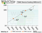
A WikiChip analysis of TSMC's next-generation 5 nanometer N5P silicon fabrication node estimates a massive 84-87% increase in transistor densities on offer compared to the company's first commercial 7 nm-class node, the N7 (7 nm DUV). The report estimates an 87% transistor-density increase, even though TSMC's own figure is slightly modest, at 84%. TSMC N5P node is expected to commence production later this year. Its precursor, TSMC N5, began risk production earlier this year, with production on the node commencing in April or May, unless derailed by the COVID-19 pandemic. The N5P node provides transistor densities of an estimated 171.3 million transistors per mm² die area, compared to 91.2 mTr/mm² of N7. Apple is expected to be the node's biggest customer in 2020, with the company building its A14-series SoC on it.
Xbox Series X Semi-custom SoC Features 320-bit Memory Interface, 10 GB or 20 GB Memory

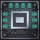
Microsoft's upcoming Xbox Series X entertainment system is shaping up to be a technological monstrosity. Xbox group head at Microsoft, Phil Spencer, last revealed a picture of its semi-custom SoC back in January, by setting it as his Twitter display picture. Over the following weeks, many more technical details, such as the chip's 12 TFLOP/s combined compute power, would be let out. Spencer updated his display picture revealing a segment of the Xbox Series X mainboard with the SoC and memory chips surrounding it. The picture reveals the large SoC package in the center, surrounded on three sides by ten memory chips, possibly GDDR6, each with its own wiring to the SoC. This indicates that the SoC features a 320-bit wide memory interface.

As for the memory density, there's no way to tell. It could be 10 GB if those are 8 Gbit memory chips, or 20 GB if those are 16 Gbit. It boils down to which device the Xbox Series X the company wants to succeed. The Xbox One S features 8 GB of DDR3, while the spruced up Xbox One X features 12 GB of GDDR5. If the new Xbox Series X succeeds the latter, then it could very well feature 20 GB, more so given Microsoft's lofty design goals (4K UHD gaming with real-time ray-tracing). Microsoft leverages hUMA to use a common memory pool for both the CPU and GPU. Designed in collaboration with AMD on a TSMC 7 nm-class node (likely the N7P), the SoC features "Zen 2" CPU cores, and a GPU based on the RDNA2 graphics architecture.
Xbox Series X memory

Xbox Head Posts "Project Scarlett" (Xbox Series X) SoC Picture, Has that 7nm Tinge

Phil Spencer, head of the Xbox division at Microsoft, posted a picture of the semi-custom SoC at the heart of the company's upcoming "Project Scarlett" Xbox Series X game console as his Twitter avatar. The picture reveals a chip that looks visibly similar to that of "Project Scorpio" (Xbox One X). The picture was also taken from an angle that reveals the pinkish/auburn tinge of 7 nm AMD chips made at TSMC. You'll find the same tinge on chips such as "Navi 10" when viewed from an angle. The die unabashedly bears the "Project Scarlett" and "8K" markings.

Next-generation game consoles are marketing 4K 60 Hz and 8K gaming capability. They likely use a combination of dynamic resolution-scale and variable rate shading to achieve this. The "Project Scarlett" SoC is a semi-custom chip co-designed by Microsoft and AMD, and uses CPU cores based on the company's "Zen 2" microarchitecture, combined with a powerful GPU based on RDNA2, which features hardware-accelerated ray-tracing and variable-rate shading. Hardware enthusiasts on Twitter are abuzz with estimating the die-size of the SoC, with calculations pinning it around the 350 mm² mark ±10 mm², or roughly similar to that of "Project Scorpio," but one must factor in the switch to 7 nm from 16 nm significantly increasing transistor-density.

AMD to Outpace Apple as TSMC's Biggest 7nm Customer in 2020

AMD in the second half of 2020 could outpace Apple as the biggest foundry customer of TSMC for its 7 nm silicon fabrication nodes (DUV and EUV combined). There are two key factors contributing to this: AMD significantly increasing its orders for the year; and Apple transitioning to TSMC's 5 nm node for its A14 SoC, freeing up some 7 nm allocation, which AMD grabbed. AMD is currently tapping into 7 nm DUV for its "Zen 2" chiplet, "Navi 10," and "Navi 14" GPU dies. The company could continue to order 7 nm DUV until these products reach EOL; while also introducing the new "Renoir" APU die on the process. The foundry's new 7 nm+ (EUV) node will be utilized for "Zen 3" chiplets and "Navi 2#" GPU dies in 2020.

Currently, the top-5 customers for TSMC 7 nm are Apple, HiSilicon, Qualcomm, AMD, and MediaTek. Barring AMD, the others in the top-5 build mobile SoCs or 4G/5G modem chips on the node. AMD is expected to top the list as it scales up orders with TSMC. In the first half of 2020, TSMC's monthly output for 7 nm is expected to grow to 110,000 wafers per month (wpm). Apple's migration to 5 nm in 2H-2020, coupled with capacity-addition could take TSMC's 7 nm output to 140,000 wpm. AMD has reportedly booked the entire capacity-addition for 30,000 wpm, taking its allocation up to 21% in 2H-2020. Qualcomm is switching to Samsung for its next-generation SoCs and modems designed for 7 nm EUV. NVIDIA, too, is expected to built its next-gen 7 nm EUV GPUs on Samsung instead of TSMC. These moves by big players could free up significant foundry allocation at TSMC for AMD's volumes to grow in 2020.

ASRock Launches the Radeon RX 5500 XT Phantom Gaming D 8G OC Graphics Card

he leading global motherboard, graphics card and mini PC manufacturer, ASRock, launches the Radeon RX 5500 XT Phantom Gaming D 8G OC graphics card - as the latest member of the ASRock Phantom Gaming series graphics card product line, equipped with AMD 's 2nd generation 7nm Radeon RX 5500 XT GPU, 8 GB 128-bit GDDR6 video memory, and support PCI Express 4.0 bus standard, as well as the new dual fan design with Phantom Gaming appearance, brilliant Polychrome SYNC lighting effect synchronization, and the stylish metal backplane. The advanced specifications and rich functions bring gamers an outstanding 1080p gaming experience.

7nm Intel Xe GPUs Codenamed "Ponte Vecchio"

Intel's first Xe GPU built on the company's 7 nm silicon fabrication process will be codenamed "Ponte Vecchio," according to a VideoCardz report. These are not gaming GPUs, but rather compute accelerators designed for exascale computing, which leverage the company's CXL (Compute Express Link) interconnect that has bandwidth comparable to PCIe gen 4.0, but with scalability features slated to come out with future generations of PCIe. Intel is preparing its first enterprise compute platform featuring these accelerators codenamed "Project Aurora," in which the company will exert end-to-end control over not just the hardware stack, but also the software.

"Project Aurora" combines up to six "Ponte Vecchio" Xe accelerators with up to two Xeon multi-core processors based on the 7 nm "Sapphire Rapids" microarchitecture, and OneAPI, a unifying API that lets a single kind of machine code address both the CPU and GPU. With Intel owning the x86 machine architecture, it's likely that Xe GPUs will feature, among other things, the ability to process x86 instructions. The API will be able to push scalar workloads to the CPU, and and the GPU's scalar units, and vector workloads to the GPU's vector-optimized SIMD units. Intel's main pitch to the compute market could be significantly lowered software costs from API and machine-code unification between the CPU and GPU.
Image Courtesy: Jan Drewes

Intel CFO Talks About 7nm Rollout, Delay in 10nm, Increased Competition from AMD

Intel CFO George Davis in an interview with Barron's commented on the company's financial health, and some of the reasons behind its rather conservative gross margin guidance looking forward to at least 2023. Intel's current product stack is moving on to the company's 10 nm silicon fabrication process in a phased manner. The company is allocating 10 nm to mobile processors and enterprise processors, while brazening it out with 14 nm on the client-desktop and HEDT platforms until they can build 10 nm desktop parts. AMD has deployed its high-IPC "Zen 2" microarchitecture on TSMC's 7 nm DUV process, with plans to go EUV in the coming months.

"We're still keenly focused on gross margin. Everything from capital efficiency to the way we're designing our products. What we've said though, the delay in 10 nanometer means that we're going to be a little bit disadvantaged on unit cost for a period of time. We actually gave guidance for gross margin out in 2021 to help people understand. 2023 is the period that we were ultimately guiding [when] we're going to see very strong revenue growth and margin expansion. We've got to get through this period where we have the 10 nanometer being a little bit late [as] we're not optimized on a node that we're on. But [by] then we're moving to a two to two and a half year cadence on the next nodes. So we're pulling in the spending on 7 nanometer, which will start up in the second half of 2021 because we think it's the right thing to do competitively," he said.

TSMC Starts Shipping its 7nm+ Node Based on EUV Technology

TSMC today announced that its seven-nanometer plus (N7+), the industry's first commercially available Extreme Ultraviolet (EUV) lithography technology, is delivering customer products to market in high volume. The N7+ process with EUV technology is built on TSMC's successful 7 nm node and paves the way for 6 nm and more advanced technologies.

The N7+ volume production is one of the fastest on record. N7+, which began volume production in the second quarter of 2019, is matching yields similar to the original N7 process that has been in volume production for more than one year.

AMD Announces Availability of the Ryzen PRO 3000 Series Processors

Today, AMD announced the global availability of its new AMD Ryzen PRO 3000 Series desktop processor lineup, along with new AMD Ryzen PRO processors with Radeon Vega Graphics and AMD Athlon PRO processors with Radeon Vega Graphics. The AMD Ryzen PRO and Athlon PRO desktop processors combine powerful performance, built-in security features, and commercial-grade reliability to get the job done. Starting in Q4 2019, robust enterprise desktops from HP and Lenovo powered by AMD Ryzen PRO and Athlon PRO desktop processors are slated to be available.

"The launch of the Ryzen PRO 3000 Series processors for commercial and small business users is the latest demonstration of our commitment to technology leadership in 2019," said Saied Moshkelani, senior vice president and general manager, AMD Client Compute. "Designed specifically to efficiently data-crunch, design, compose, and create - AMD Ryzen PRO and Athlon PRO processors accelerate enhanced business productivity while offering protection safeguards with built-in security features, such as full system memory encryption and a dedicated, on-die security processor."

AMD Could Release Next Generation EPYC CPUs with Four-Way SMT

AMD has completed design phase of its "Zen 3" architecture and rumors are already appearing about its details. This time, Hardwareluxx has reported that AMD could bake a four-way simultaneous multithreading technology in its Zen 3 core to enable more performance and boost parallel processing power of its data center CPUs. Expected to arrive sometime in 2020, Zen 3 server CPUs, codenamed "MILAN", are expected to bring many architectural improvements and make use of TSMC's 7nm+ Extreme Ultra Violet lithography that brings as much as 20% increase in transistor density.

Perhaps the biggest change we could see is the addition of four-way SMT that should allow a CPU to have four virtual threads per core that will improve parallel processing power and enable data center users to run more virtual machines than ever before. Four-way SMT will theoretically boost performance by dividing micro-ops into four smaller groups so that each thread could execute part of the operation, thus making the execution time much shorter. This being only one application of four-way SMT, we can expect AMD to leverage this feature in a way that is most practical and brings the best performance possible.

BIOSTAR Launches the New X470MH Motherboard

BIOSTAR, a leading manufacturer of motherboards, graphics cards, and storage devices, is proud to announce a new addition to its AMD socket AM4 motherboards with the BIOSTAR X470MH. Built for office workers looking to smoothly cruise through their daily tasks without setbacks and for home users looking for a strong and stable platform to run their HTPC, the X470MH is equipped with the latest features the PC industry has to offer while maintaining an affordable price point. And for those looking to push the limit, the X470MH offers overclocking possibilities giving the user the added performance benefit for faster gaming and task management without risking to damage their investment.

The BIOSTAR X470MH, equipped with AMD's X470 chipset and AMD AM4 CPU socket, brings support for AMD's latest 3rd Gen Ryzen 7 nm processors. Built to make your daily computer needs a breeze, the X470MH is a Micro ATX motherboard featuring USB 3.1 Gen1 support (5 Gb/s) providing fast transfer speeds and support to a wide array of peripherals, PCI-e M.2 at 32 Gb/s for increased system responsiveness, as well as HDMI 4K resolution to sooth the eye while watching Netflix or Youtube, and a VGA port for a wider range of monitor compatibility. In addition, the Internet and network connectivity will not be a drag with the onboard Realtek GbE LAN. Overclockers are not left out either with enough room for 2x DDR4 RAM slots which support up to 32 GB and overclocks at 3200 MHz, making multitasking a pleasant experience.

AMD Designing Zen 4 for 2021, Zen 3 Completes Design Phase, out in 2020

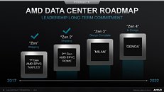
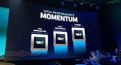
AMD in its 2nd generation EPYC processor launch event announced that it has completed the design phase of its next-generation "Zen 3" CPU microarchitecture, and is currently working on its successor, the "Zen 4." AMD debuted its "Zen 2" microarchitecture with the client-segment 3rd generation Ryzen desktop processor family, it made its enterprise debut with the 2nd generation EPYC. This is the first x86 CPU microarchitecture designed for the 7 nanometer silicon fabrication process, and is being built on a 7 nm DUV (deep ultraviolet) node at TSMC. It brings about double-digit percentage IPC improvements over "Zen+."

The "Zen 3" microarchitecture is designed for the next big process technology change within 7 nm, EUV (extreme ultraviolet), which allows significant increases in transistor densities, and could facilitate big improvements in energy-efficiency that could be leveraged to increase clock-speeds and performance. It could also feature new ISA instruction-sets. With "Zen 3" passing design phase, AMD will work on prototyping and testing it. The first "Zen 3" products could debut in 2020. "Zen 4" is being designed for a different era.

AMD Reports Second Quarter 2019 Financial Results

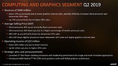
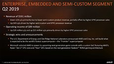
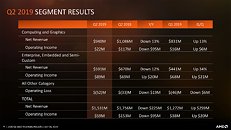
AMD (NASDAQ:AMD) today announced revenue for the second quarter of 2019 of $1.53 billion, operating income of $59 million, net income of $35 million and diluted earnings per share of $0.03. On a non-GAAP basis, operating income was $111 million, net income was $92 million and diluted earnings per share was $0.08.

"I am pleased with our financial performance and execution in the quarter as we ramped production of three leadership 7nm product families," said Dr. Lisa Su, AMD president and CEO. "We have reached a significant inflection point for the company as our new Ryzen, Radeon and EPYC processors form the most competitive product portfolio in our history and are well positioned to drive significant growth in the second half of the year."

AMD Readies Larger 7nm "Navi 12" Silicon to Power Radeon RX 5800 Series?

AMD is developing a larger GPU based on its new "Navi" architecture to power a new high-end graphics card family, likely the Radeon RX 5800 series. The codename "Navi 12" is doing rounds on social media through familiar accounts that have high credibility with pre-launch news and rumors. The "Navi 10" silicon was designed to compete with NVIDIA's "TU106," as its "XT" and "Pro" variants outperform NVIDIA's original RTX 2060 and RTX 2070, forcing it to develop the RTX 20 Super series, by moving up specifications a notch.

Refreshing its $500 price-point was particularly costly for NVIDIA, as it was forced to tap into the 13.6 billion-transistor "TU104" silicon to carve out the RTX 2070 Super; while for the RTX 2060 Super, it had to spend 33 percent more on the memory chips. With the "Navi 12" silicon, AMD is probably looking to take a swing at NVIDIA's "TU104" silicon, which has been maxed out by the RTX 2080 Super, disrupting the company's $500-700 lineup once again, with its XT and Pro variants. There's also a remote possibility of "Navi 12" being an even bigger chip, targeting the "TU102."

BIOSTAR Launches the Newest AMD Radeon RX5700XT and RX5700 Graphics Cards

BIOSTAR, a leading manufacturer of motherboards, graphics cards, and storage devices, welcomes the arrival of PCI Express 4.0 with the AMD Radeon RX5700-series of graphics cards, the world's first graphics cards to support the 4th generation PCI Express interface. BIOSTAR is proudly launching its first Radeon RX5700-series cards, namely the Radeon RX5700XT and Radeon RX5700. Beyond gaining twice the PCI-E bandwidth compared to previous generations of graphics cards, the Radeon RX5700-series also features the first mass market 7nm GPU. It's also AMD's first GPU based on their brand new RDNA architecture. Another first is support for GDDR6 memory, which offers twice the peak bandwidth compared to GDDR5.

AMD's RDNA architecture is a completely new GPU design that brings a wide range of new features to the Radeon RX5700-series, such as a streamlined graphics pipeline, a brand new compute unit design and a multilevel cache hierarchy. Together, things bring a 50% performance per Watt advantage over AMD's previous GCN architecture.

PowerColor Announces the Radeon RX 5700 Series

TUL Corporation, a leading and innovative manufacturer of AMD graphic cards since 1997, has introduced its newest series, the PowerColor RX 5700 and PowerColor RX 5700 XT, the world's first PCIe 4.0 GPU for the most demanding 1440p gaming with the most advanced gaming technology. Using the newest AMD RDNA architecture, the PowerColor RX 5700 and RX 5700 XT shows impressive performance improvements as well vastly improved performance per watt over the previous generations with the GPU being manufactured with the leading edge 7nm process.

With the new RDNA architecture, PowerColor RX 5700 and RX 5700 XT was engineered to greatly enhance gaming using features like Radeon Image Sharpening, FidelityFX for maximum performance and insane immersive gaming experiences as well the new Radeon Anti-Lag, stutter-free, tear-free gaming with AMD Radeon FreeSync technology, for incredibly responsive gameplay.

Sapphire Announces its Radeon RX 5700 XT and RX 5700 Reference Graphics Cards

Great gaming experiences are created by bending the rules. The new SAPPHIRE Radeon RX 5700 Series GPUs, powered by RDNA architecture, are designed from the ground up for superb 1440p performance and exceptional power efficiency for high-fidelity gaming. The Radeon RX 5700 Series GPUs house AMD's 2nd generation 7nm architecture, 8GB of GDDR6 high-speed memory and PCI Express 4.0 support. These GPUs are impeccably engineered to exponentially reduce lag, increase efficiency and surround you in immersive stutter-free gameplay.

The Radeon RX 5700 XT GPU bends the rules with a revolutionary metal exoskeleton for heat dissipation, fused with the reimagined contour silhouette, and precision machined accents to perform as good as it looks.

Qualcomm and Lenovo Unveil World's First 5G PC Powered By The Qualcomm Snapdragon Processor

Qualcomm Technologies, Inc., a subsidiary of Qualcomm Incorporated, announced in conjunction with Lenovo the world's first 5G PC2 today at its Computex Press Conference. Project Limitless encompasses a strong technology collaboration between Qualcomm Technologies, Inc. a leader in 5G connectivity, and Lenovo, the leader in PCs, to bring innovation to the always on, always connected PC ecosystem. Project Limitless is powered by the Qualcomm Snapdragon 8cx 5G compute platform and is the world's first 7nm platform purpose-built for PCs that offers 5G connectivity.

The new platform is running on Windows 10 for ARM. It promises multi-day battery life and 7GBps transfer speeds with a Snapdragon x55 5G modem.
Image Source: Tom's Hardware

COLORFUL Announces First AMD X570 Motherboard with New CVN X570 GAMING PRO V14

Colorful Technology Company Limited, professional manufacturer of graphics cards, motherboards and high-performance storage solutions is thrilled to introduce its latest product to gamers, enthusiasts, power users and system builders with the release of the COLORFUL first AMD X570-based motherboard. The new COLORFUL CVN X570 GAMING PRO V14 serves as a foundation for new AMD builds and supports AM4 socket processors including 3rd Gen AMD Ryzen desktop processors.

The CVN X570 GAMING Pro is ready for the future with support for AMD's new 7nm processor based on their Zen2 architecture, while still supporting both 2nd Gen and 1st Gen Ryzen products. This provides and easier and more cost effective upgrade path into the latest hardware. Making its debut is PCIe 4.0 on this motherboard giving it extra bandwidth for high-speed connections with devices. The motherboard also comes rich with USB connectivity including USB3.1 Gen2 and also features wireless LAN.

AMD Announces Radeon RX 5700 Based on Navi: RDNA, 7nm, PCIe Gen4, GDDR6

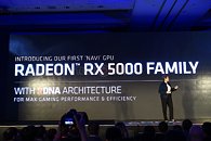
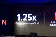
AMD at its 2019 Computex keynote today unveiled the Radeon RX 5000 family of graphics cards that leverage its new Navi graphics architecture and 7 nm silicon fabrication process. Navi isn't just an incremental upgrade over Vega with a handful new technologies, but the biggest overhaul to AMD's GPU SIMD design since Graphics CoreNext, circa 2011. Called RDNA or Radeon DNA, the new compute unit by AMD is a clean-slate SIMD design with a 1.25X IPC uplift over Vega, an overhauled on-chip cache hierarchy, and a more streamlined graphics pipeline.

In addition, the architecture is designed to increase performance-per-Watt by 50 percent over Vega. The first part to leverage Navi is the Radeon RX 5700. AMD ran a side-by-side demo of the RX 5700 versus the GeForce RTX 2070 at Strange Brigade, where NVIDIA's $500 card was beaten. "Strange Brigade" is one game where AMD fares generally well as it is heavily optimized for asynchonous compute. Navi also ticks two big technology check-boxes, PCI-Express gen 4.0, and GDDR6 memory. AMD has planned a July availability for the RX 5700, and did not disclose pricing.

Samsung Announces Breakthrough in Building Blocks of 3nm Circuits, Updates Roadmap

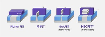
Samsung Electronics Co., Ltd., a world leader in advanced semiconductor technology, today announced its ongoing commitment to foundry innovation and service at the Samsung Foundry Forum 2019 USA, providing the silicon community with wide-ranging updates on technology advances that support the most demanding applications of today and tomorrow.

The event, held today in Santa Clara, California, features top Samsung executives and industry experts reviewing progress on semiconductor technologies and foundry platform solutions that enable developments in artificial intelligence (AI), machine learning, 5G networking, automotive, the Internet of Things (IoT), advanced data centers and many other domains.

Intel Switches to a "Data Center First" Strategy with 7nm

Intel traditionally released new CPU microarchitectures and new silicon fabrication nodes with the client segment, and upon observing some degree of maturity with both, graduated them to the enterprise segment. With its homebrew 7 nanometer silicon fabrication process that takes flight in 2021, Intel will flip its roadmap execution strategy, by going "Data Center First." Speaking at the 2019 Investors Day summit, Intel SVP and GM of Data Center Group Navin Shenoy revealed that the first product built on Intel's 7 nm process will be a GPGPU accelerator chip derived from the Xe architecture for the Data Center, followed closely by a new server CPU. Both these products come under Shenoy's group. One is a competitor to likes of NVIDIA Tesla and AMD Radeon Instinct, while the other is a Xeon processor competing with AMD EPYC.

Shenoy explained the reason why within his group, the GPGPU product was prioritized over the server CPU. It has to do with redundancy of the GPU silicon, or specifically, the higher potential to harvest partially defective dies than CPU. A GPU has a larger number of indivisible components that can be disabled if found non-functional at the time of quality assurance, and these harvested dies can be used to carve out variants of a main product. An example of this would be NVIDIA carving out the GeForce GTX 1070 (1,920 CUDA cores) from the GP104 silicon that physically has 2,560 CUDA cores. The first manufacturing runs of the GPGPU will give the foundry valuable insights into the way the node is behaving, so it could be refined and matured for the server CPU. With 10 nm, however, Intel is sticking to the client-first model, by rolling out the "Ice Lake" processor towards the end of 2019. Within the Client Computing group, Intel has flipped its roadmap execution such that mobile (notebook) CPUs take precedence over desktop ones.

Intel Switches Gears to 7nm Post 10nm, First Node Live in 2021

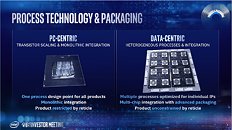
Intel's semiconductor manufacturing business has had a terrible past 5 years as it struggled to execute its 10 nanometer roadmap forcing the company's processor designers to re-hash the "Skylake" microarchitecture for 5 generations of Core processors, including the upcoming "Comet Lake." Its truly next-generation microarchitecture, codenamed "Ice Lake," which features a new CPU core design called "Sunny Cove," comes out toward the end of 2019, with desktop rollouts expected 2020. It turns out that the 10 nm process it's designed for, will have a rather short reign at Intel's fabs. Speaking at an investor's summit on Wednesday, Intel put out its silicon fabrication roadmap that sees an accelerated roll-out of Intel's own 7 nm process.

When it goes live and fit for mass production some time in 2021, Intel's 7 nm process will be a staggering 3 years behind TSMC, which fired up its 7 nm node in 2018. AMD is already mass-producing CPUs and GPUs on this node. Unlike TSMC, Intel will implement EUV (extreme ultraviolet) lithography straightaway. TSMC began 7 nm with DUV (deep ultraviolet) in 2018, and its EUV node went live in March. Samsung's 7 nm EUV node went up last October. Intel's roadmap doesn't show a leap from its current 10 nm node to 7 nm EUV, though. Intel will refine the 10 nm node to squeeze out energy-efficiency, with a refreshed 10 nm+ node that goes live some time in 2020.

TSMC Unveils 6-nanometer Process

TSMC today announced its 6-nanometer (N6) process, which provides a significant enhancement of its industry-leading N7 technology and offers customers a highly competitive performance-to-cost advantage as well as fast time-to-market with direct migration from N7-based designs. By leveraging the new capabilities in extreme ultraviolet (EUV) lithography gained from the N7+ technology currently in risk production, TSMC's N6 process delivers 18% higher logic density over the N7 process. At the same time, its design rules are fully compatible with TSMC's proven N7 technology, allowing its comprehensive design ecosystem to be reused. As a result, it offers a seamless migration path with a fast design cycle time with very limited engineering resources for customers to achieve the product benefits from the new technology offering.

Scheduled for risk production in the first quarter of 2020, TSMC's N6 technology provides customers with additional cost-effective benefits while extending the industry-leading power and performance from the 7nm family for a broad array of applications, ranging from high-to-mid end mobile, consumer applications, AI, networking, 5G infrastructure, GPU, and high-performance computing.

AMD Zen3 to Leverage 7nm+ EUV For 20% Transistor Density Increase

AMD "Zen 3" microarchitecture could be designed for the enhanced 7 nm+ EUV (extreme ultraviolet) silicon fabrication node at TSMC, which promises a significant 20 percent increase in transistor densities compared to the 7 nm DUV (deep ultraviolet) node on which its "Zen 2" processors are being built. In addition, the node will also reduce power consumption by up to 10 percent at the same operational load. In a late-2018 interview, CTO Mark Papermaster stated AMD's design goal with "Zen 3" would be to prioritize energy-efficiency, and that it would present "modest" performance improvements (read: IPC improvements) over "Zen 2." AMD made it clear that it won't drag 7 nm DUV over more than one microarchitecture (Zen 2), and that "Zen 3" will debut in 2020 on 7 nm+ EUV.
Return to Keyword Browsing
Dec 18th, 2024 17:31 EST change timezone

New Forum Posts

Popular Reviews

Controversial News Posts