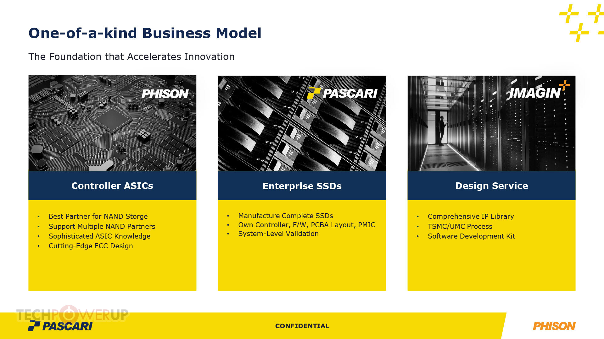
Phison Announces Pascari Brand of Enterprise SSDs, Debuts X200 Series Across Key Form-factors
Phison is arguably the most popular brand for SSD controllers in the client segment, but is turning more of attention to the vast enterprise segment. The company had been making first-party enterprise SSDs under its main marquee, but decided that the lineup needed its own brand that enterprise customers could better discern from the controller ASIC main brand. We hence have Pascari and Imagin. Pascari is an entire product family of fully built enterprise SSDs from Phison. The company's existing first-party drives under the main brand will probably migrate to the Pascari catalog. Imagin, on the other hand, is a design service for large cloud and data-center customers, so they could develop bespoke tiered storage solutions at scale.
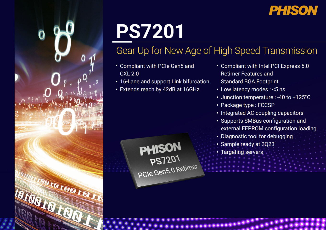
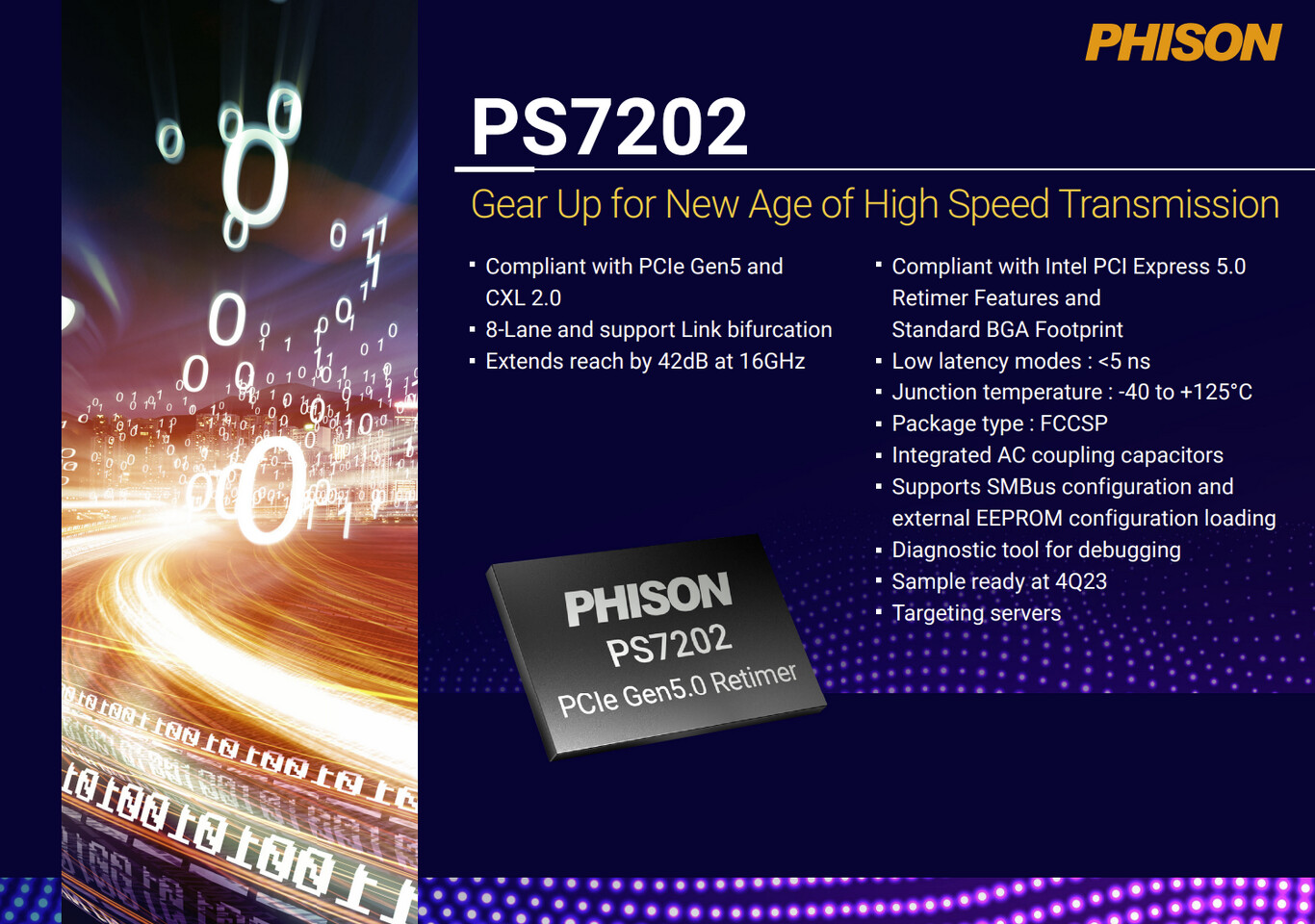
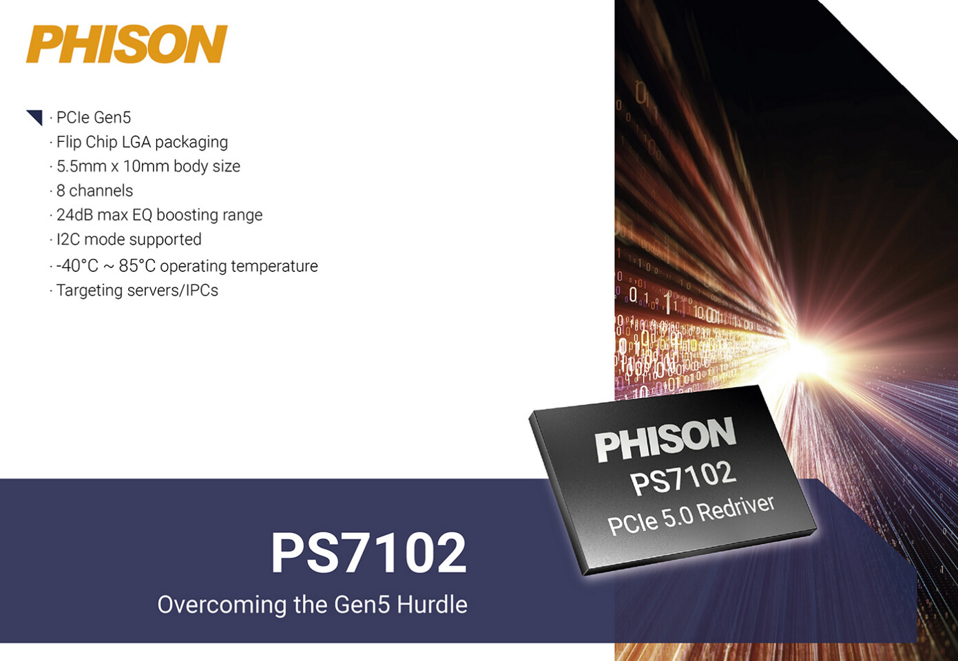
The Pascari line of enterprise SSDs are designed completely in-house by Phison, feature their latest controllers, firmware, PCB, PMIC, and on-device power-failure protection on select products. The third-party components here are the NAND flash and DRAM chips, which have both been thoroughly evaluated by Phison for the best performance, endurance, and reliability, at their enterprise SSD design facility in Broomfield, Colorado. Phison already had a constellation of industry partners and suppliers to go around with, and the company's drives even power space missions; but the Pascari brand better differentiates the fully-built SSD lineup from the ASIC make. Pascari makes its debut with the X200 series high-performance SSDs for high-access heat data. The drive leverages Phison's latest PCIe Gen 5 controller technology, the most optimized memory components, and availability in all contemporary server storage form-factors.


The Pascari line of enterprise SSDs are designed completely in-house by Phison, feature their latest controllers, firmware, PCB, PMIC, and on-device power-failure protection on select products. The third-party components here are the NAND flash and DRAM chips, which have both been thoroughly evaluated by Phison for the best performance, endurance, and reliability, at their enterprise SSD design facility in Broomfield, Colorado. Phison already had a constellation of industry partners and suppliers to go around with, and the company's drives even power space missions; but the Pascari brand better differentiates the fully-built SSD lineup from the ASIC make. Pascari makes its debut with the X200 series high-performance SSDs for high-access heat data. The drive leverages Phison's latest PCIe Gen 5 controller technology, the most optimized memory components, and availability in all contemporary server storage form-factors.