News Posts matching #Ampere

Return to Keyword Browsing

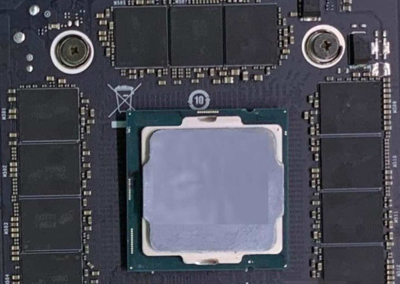
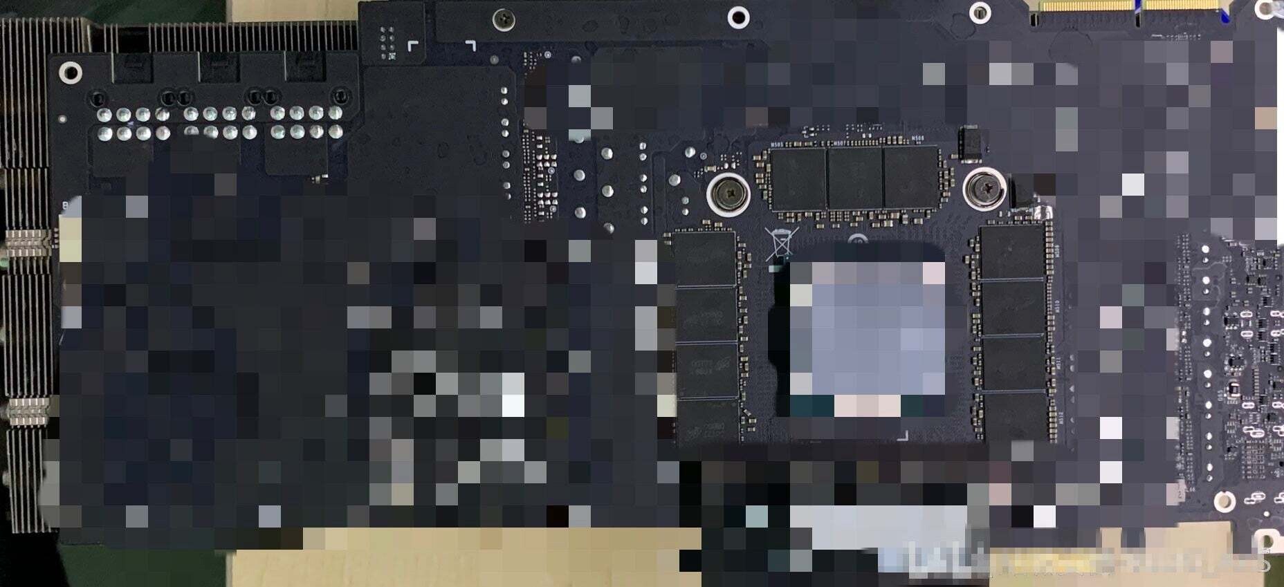
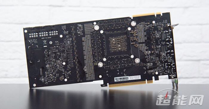
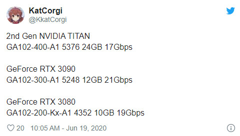
NVIDIA Ampere GA102-300-A1 GPU Die Pictured

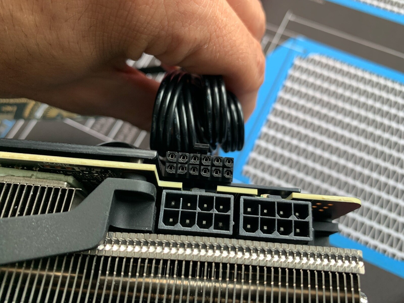
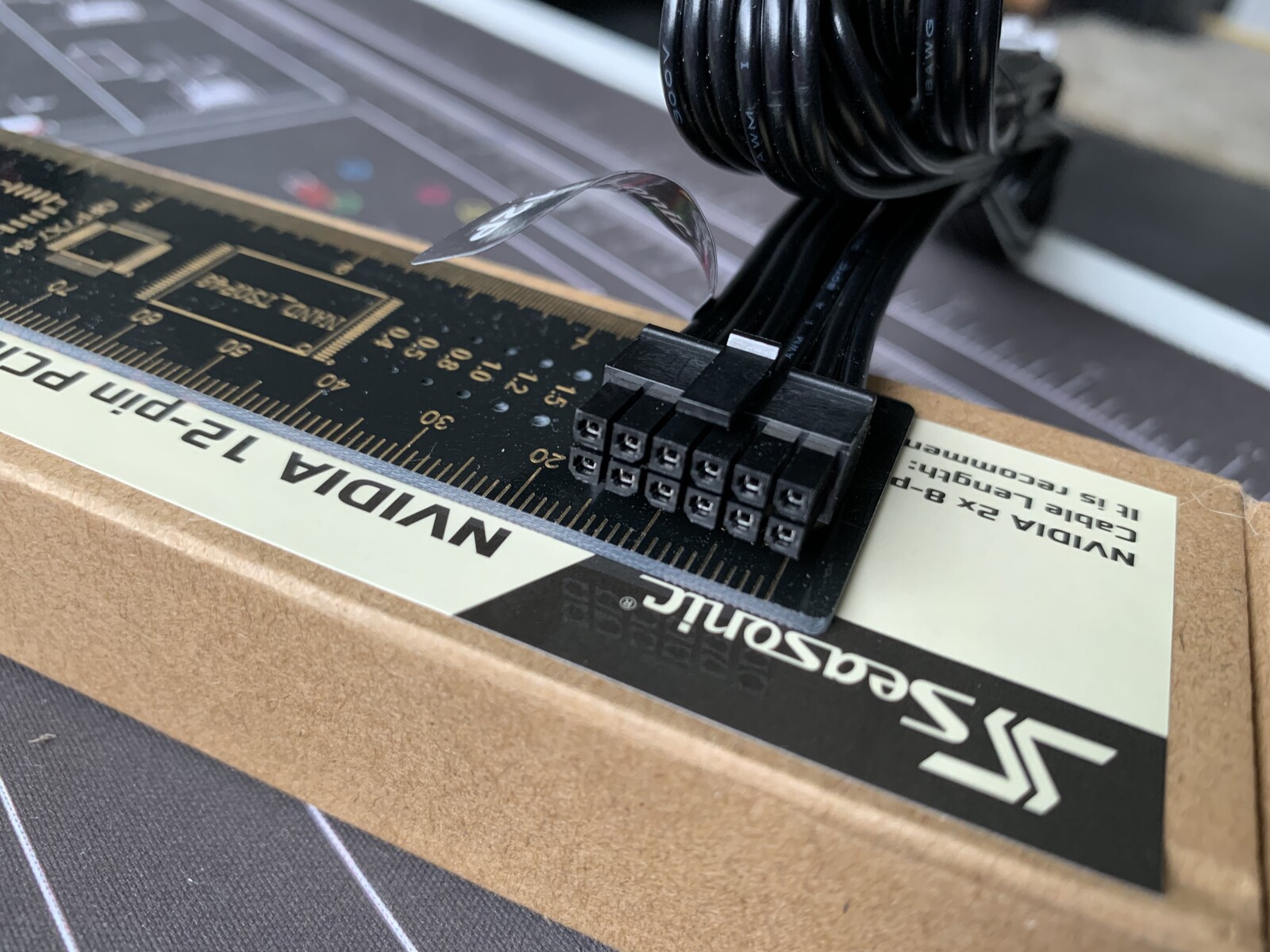
Here's the first picture of an NVIDIA "Ampere" GA102 GPU die. This is the largest client-segment implementation of the "Ampere" architecture by NVIDIA, targeting the gaming (GeForce) and professional-visualization (Quadro) market segments. The "Ampere" architecture itself debuted earlier this year with the A100 Tensor Core scalar processor that's winning hearts and minds in the HPC community faster than ice cream on a dog day afternoon. There's no indication of die-size, but considering how tiny the 10.3 billion-transistor AMD "Navi 10" die is, the GA102 could come with a massive transistor count if its die is as big as that of the TU102. The GPU in the picture is also a qualification sample, and was probably pictured off a prototype graphics card. Powering the GeForce RTX 3090, the GA102-300 is expected to feature a CUDA core count of 5,248. According to VideoCardz, there's a higher trim of this silicon, the GA102-400, which could make it to NVIDIA's next halo product under the TITAN brand.

NVIDIA 12-pin Connector Pictured Next to 8-pin PCIe - It's Tiny

Over the weekend, we got some of the first pictures of a production-grade NVIDIA 12-pin graphics card power connector that debuts with the company's GeForce "Ampere" Founders Edition graphics cards. HardwareLuxx.de received a set of modular cables by Seasonic that can be plugged into the company's modular PSUs, directly putting out a 12-pin connector. The publication's editor Andreas Schilling posted this striking picture that is sure to change our perspective about the 12-pin connector - it is tiny!

Called the Molex Micro-Fit 3.0 12-pin connector, the NVIDIA 12-pin connector looks visibly smaller than a single 8-pin PCIe power connector, and only slightly broader. It yet uses high gauge wires and pins, so it can push up to 600 W of power - more power than two 8-pin connectors. The space-saving connector shouldn't just be easier to plug in, but also cable-manage, since you're only having to wrestle with one cable, even for a high-end graphics card. Not only is the connector NVIDIA-exclusive, but there are also indications that only the Founders Edition (reference design) GeForce "Ampere" cards feature it, while custom-design cards based on the GPUs make do with a bunch of 8-pin PCIe power connectors.

Ampere's Launch Edges Closer: NVIDIA "PG133A" Board Gets RRA Certification

That Ampere's launch is edging closer is sort of a lapalissian truth; as time advances, a new consumer gaming graphics card from NVIDIA becomes ever more likely. However, we are now witnessing what amount to be the final steps in NVIDIA's preparation for launch of their next-generation RTX 3000 series. NVIDIA has submitted with the Korean National Radio Research Agency (RAA) their PG133A board design for certification, which is being pegged as the one that's been in numerous leaks already, with that fancy PCB and cooling solution.

Such certification is one of the last steps before a product comes to market, and timing seems to be inline with the #ultimatecountdown teaser that NVIDIA has been spearheading, the results of which should be clear by August 31st. It remains to be seen if the Founders' Edition will feature the leaked cooler across all products, of if NVIDIA will be staggering its design (maybe re-purposing that of last year's RTX 2000 series) for lower-tier SKUs in order to shave costs.

NVIDIA Announces GTC 2020 Keynote to be Held on October 5-9

NVIDIA today announced that it will be hosting another GTC keynote for the coming month of October. To be held between October 5th and October 9th, the now announced keynote will bring updates to NVIDIA's products and technologies, as well as provide an opportunity for numerous computer science companies and individuals to take center stage on discussing new and upcoming technologies. More than 500 sessions will form the backbone of GTC, with seven separate programming streams running across North America, Europe, Israel, India, Taiwan, Japan and Korea - each with access to live demos, specialized content, local startups and sponsors.

This GTC keynote follows the May 2020 keynote where the world was presented to NVIDIA's Ampere-based GA100 accelerator. A gaming and consumer-oriented event is also taking place on September 1st, with expectations being set high for NVIDIA's next-generation of consumer graphics products. Although if recent rumors of a $2,000 RTX 3090 graphics card are anything to go by, not only expectations will be soaring by then.

NVIDIA GeForce RTX 3080 Surfaces on Userbenchmark, Rocks 19Gbps Memory Clock

NVIDIA's second fastest "Ampere" graphics card to launch this year, the GeForce RTX 3080, surfaced on the Userbenchmark database. Hardware Leaks (aka @_rogame) fished out several juicy details about the card that will be positioned right below the flagship RTX 3090 (RTX 2080 Ti successor) that's been in the news lately. The RTX 3080 succeeds the RTX 2080. On the Userbenchmark database, the purported RTX 3080 is shown bearing a device ID "10DE 2206." Among its readable specs leaked are a GPU frequency of up to 2.10 GHz, possibly frequency capped just like "Turing," and 10 GB of GDDR6X memory across a 320-bit wide memory interface, and a memory clock speed of 19 Gbps (GDDR6X effective), which works out to 760 GB/s of memory bandwidth.

NVIDIA GeForce RTX 3090 "Ampere" Alleged PCB Picture Surfaces

As we are getting close to September 1st, the day NVIDIA launches its upcoming GeForce RTX graphics cards based on Ampere architecture, we are getting even more leaks. Today, an alleged PCB of the NVIDIA's upcoming GeForce RTX 3090 has been pictured and posted on social media. The PCB appears to be a 3rd party design coming from one of NVIDIA's add-in board (AIB) partners - Colorful. The picture is blurred out on the most of the PCB and has Intel CPU covering the GPU die area to hide the information. There are 11 GDDR6X memory modules covering the surrounding of the GPU and being very near it. Another notable difference is the NVLink finger change, as there seems to be the new design present. Check out the screenshot of the Reddit thread and PCB pictures below:
NVIDIA GeForce RTX 3090 PCB NVIDIA GeForce RTX 3090 PCB NVIDIA GeForce RTX 3090 PCB
More pictures follow:

Custom-design NVIDIA Ampere Cards to Launch Alongside Founders Edition Cards

In signs of NVIDIA's upcoming GeForce Ampere graphics cards getting a brisk market launch across several SKUs, a Tweaktown report predicts that custom-design graphics cards based on the chips will launch alongside Founders Edition (de facto reference-design) cards. NVIDIA's add-in card partners are believed to be ready with their next-generation original designs that will debut with the new chips, with renders of the ASUS ROG Strix 3000-series cards having leaked in early June. Tweaktown predicts series reveal by September 9, followed by SKU announcements on September 17. AIC partners tell them that custom-design products can be expected within the month. The first major teaser could come out by August 31.

NVIDIA on Monday tweeted its very first web teaser of the new series, under the hashtag #UltimateCountdown. We predict DirectX 12 Ultimate to be central to NVIDIA's marketing, especially a play on the word "ultimate," (eg: the "ultimate ray-tracing performance"). It wouldn't surprise us if "Ultimate" is somehow integrated into the product branding itself (à la "RTX").

NVIDIA Starts Ampere Marketing With #Ultimatecountdown

NVIDIA today shared the first real teaser in what seems to be the start of the Ampere marketing push. A post via Twitter shared an image showing an explosion of cosmic proportions, with a "#theultimatecountdown" tag alongside the "21 days. 21 years" tagline. This is a likely throwback to August 31st 1999, when NVIDIA launched its first GeForce branded graphics card - the GeForce 256 - setting it on its journey to become today's most successful dedicated graphics card maker.

Following the teasers' logic, we should expect some very interesting announcements from NVIDIA come August 31st, 2020 - and with Ampere around the corner, it's highly unlikely we'll be hearing about anything other than that.

Video Memory Sizes Set to Swell as NVIDIA Readies 20GB and 24GB GeForce Amperes

NVIDIA's GeForce RTX 20-series "Turing" graphics card series did not increase video memory sizes in comparison to GeForce GTX 10-series "Pascal," although the memory itself is faster on account of GDDR6. This could change with the GeForce RTX 30-series "Ampere," as the company looks to increase memory sizes across the board in a bid to shore up ray-tracing performance. WCCFTech has learned that in addition to a variety of strange new memory bus widths, such as 320-bit, NVIDIA could introduce certain higher variants of its RTX 30-series cards with video memory sizes as high as 20 GB and 24 GB.

Memory sizes of 20 GB or 24 GB aren't new for NVIDIA's professional-segment Quadro products, but it's certainly new for GeForce, with only the company's TITAN-series products breaking the 20 GB-mark at prices due north of $2,000. Much of NVIDIA's high-end appears to be resting on segmentation of the PG132 common board design, coupled with the GA102 silicon, from which the company could carve out several SKUs spaced far apart in the company's product stack. NVIDIA's next-generation GeForce "Ampere" family is expected to debut in September 2020, with product launches in the higher-end running through late-Q3 and Q4 of 2020.

Possible NVIDIA RTX 3000 Rollout Schedule Detailed - RTX 3070 and RTX 3060 After September

September is emerging as a busy month for PC hardware announcements - if not actual product launches or availability. A report by Chinese tech publication MyDrivers suggests that the upcoming GeForce RTX 3000 series "Ampere" graphics cards could have a staggered market availability. Although the technology and product family is expected to be announced in September 17, 2020, the month could see the release of only the top-dog (read: low volume) parts, namely the flagship RTX 3080 Ti and RTX 3080 (or the SKUs that succeed the RTX 2080 Ti and RTX 2080).

The GeForce RTX 3070, or the SKU that succeeds the RTX 2070 Super, could launch a month later, in October 2020, according to the MyDrivers report. The higher-volume performance-segment part, the RTX 3060, or the SKU that succeeds the RTX 2060, could launch only by November, just in time for the Holiday shopping season. The report goes on to state that NVIDIA has discontinued production of the popular RTX 2070 Super, following its decision to stop RTX 2080 Ti and RTX 2080 Super production, allowing the retail channel to digest existing inventories of these parts.

AMD Radeon MI100 "Arcturus" Alleged Specification Listed, the GPU Could be Coming in December

AMD has been preparing to launch its MI100 accelerator and fight NVIDIA's A100 Ampere GPU in machine learning and AI horizon, and generally compute-intensive workloads. According to some news sources over at AdoredTV, the GPU alleged specifications were listed, along with some slides about the GPU which should be presented at the launch. So to start, this is what we have on the new Radeon MI100 "Arcturus" GPU based on CDNA architecture. The alleged specifications mention that the GPU will feature 120 Compute Units (CUs), meaning that if the GPU keeps the 64-core per CU configuration, we are looking at 7680 cores powered by CDNA architecture.

The leaked slide mentions that the GPU can put out as much as 42 TeraFLOPs of FP32, single-precision compute. This makes it more than twice as fast compared to NVIDIA's A100 GPU at FP32 workloads. To achieve that, the card would need to have all of its 7680 cores running at 2.75 GHz, which would be a bit high number. On the same slide, the GPU is claimed to have 9.5 TeraFLOPs of FP64 dual-precision performance, while the FP16 power is going to be around 150 TeraFLOPs. For comparison, the A100 GPU from NVIDIA features 9.7 TeraFLOPS of FP64, 19.5 TeraFLOPS of FP32, and 312 (or 634 with sparsity enabled) TeraFLOPs of FP16 compute. AMD GPU is allegedly only more powerful for FP32 workloads, where it outperforms the NVIDIA card by 2.4 times. And if that is really the case, AMD has found its niche in the HPC sector, and it plans to dominate there. According to AdoredTV sources, the GPU could be coming in December of this year.

NVIDIA A100 Ampere GPU Benchmarked on MLPerf

When NVIDIA announced its Ampere lineup of the graphics cards, the A100 GPU was there to represent the higher performance of the lineup. The GPU is optimized for heavy computing workloads as well as machine learning and AI tasks. Today, NVIDIA has submitted the MLPerf results on the A100 GPU to the MLPerf database. What is MLPerf and why it matters you might think? Well, MLPerf is a system benchmark designed to test the capability of a system for machine learning tasks and enable comparability between systems. The A100 GPU got benchmarked in the latest 0.7 version of the benchmark.

The baseline for the results was the previous generation king, V100 Volta GPU. The new A100 GPU is average 1.5 to 2.5 times faster compared to V100. So far A100 GPU system beats all offers available. It is worth pointing out that not all competing systems have been submitted, however, so far the A100 GPU is the fastest.
The performance results follow:

TSMC Allocation the Next Battleground for Intel, AMD, and Possibly NVIDIA

With its own 7 nm-class silicon fabrication node nowhere in sight for its processors, at least not until 2022-23, Intel is seeking out third-party semiconductor foundries to support its ambitious discrete GPU and scalar compute processor lineup under the Xe brand. A Taiwanese newspaper article interpreted by Chiakokhua provides a fascinating insight to the the new precious resource in the high-technology industry - allocation.

TSMC is one of these foundries, and will give Intel access to a refined 7 nm-class node, either the N7P or N7+, for some of its Xe scalar compute processors. The company could also seek out nodelets such as the N6. Trouble is, Intel will be locking horns with the likes of AMD for precious foundry allocation. NVIDIA too has secured a certain allocation of TSMC 7 nm for some of its upcoming "Ampere" GPUs. Sources tell China Times that TSMC will commence mass-production of Intel silicon as early as 2021, on either N7P, N7+, or N6. Business from Intel is timely for TSMC as it is losing orders from HiSilicon (Huawei) in wake of the prevailing geopolitical climate.

NVIDIA Ampere A100 GPU Gets Benchmark and Takes the Crown of the Fastest GPU in the World

When NVIDIA introduced its Ampere A100 GPU, it was said to be the company's fastest creation yet. However, we didn't know how fast the GPU exactly is. With the whopping 6912 CUDA cores, the GPU can pack all that on a 7 nm die with 54 billion transistors. Paired with 40 GB of super-fast HBM2E memory with a bandwidth of 1555 GB/s, the GPU is set to be a good performer. And how fast it exactly is you might wonder? Well, thanks to the Jules Urbach, the CEO of OTOY, a software developer and maker of OctaneRender software, we have the first benchmark of the Ampere A100 GPU.

Scoring 446 points in OctaneBench, a benchmark for OctaneRender, the Ampere GPU takes the crown of the world's fastest GPU. The GeForce RTX 2080 Ti GPU scores 302 points, which makes the A100 GPU up to 47.7% faster than Turing. However, the fastest Turing card found in the benchmark database is the Quadro RTX 8000, which scored 328 points, showing that Turing is still holding well. The result of Ampere A100 was running with RTX turned off, which could yield additional performance if RTX was turned on and that part of the silicon started working.

The Curious Case of the 12-pin Power Connector: It's Real and Coming with NVIDIA Ampere GPUs

Over the past few days, we've heard chatter about a new 12-pin PCIe power connector for graphics cards being introduced, particularly from Chinese language publication FCPowerUp, including a picture of the connector itself. Igor's Lab also did an in-depth technical breakdown of the connector. TechPowerUp has some new information on this from a well placed industry source. The connector is real, and will be introduced with NVIDIA's next-generation "Ampere" graphics cards. The connector appears to be NVIDIA's brain-child, and not that of any other IP- or trading group, such as the PCI-SIG, Molex or Intel. The connector was designed in response to two market realities - that high-end graphics cards inevitably need two power connectors; and it would be neater for consumers to have a single cable than having to wrestle with two; and that lower-end (<225 W) graphics cards can make do with one 8-pin or 6-pin connector.

The new NVIDIA 12-pin connector has six 12 V and six ground pins. Its designers specify higher quality contacts both on the male and female ends, which can handle higher current than the pins on 8-pin/6-pin PCIe power connectors. Depending on the PSU vendor, the 12-pin connector can even split in the middle into two 6-pin, and could be marketed as "6+6 pin." The point of contact between the two 6-pin halves are kept leveled so they align seamlessly.

NVIDIA Prepares to Stop Production of Popular RTX 20-series SKUs, Raise Prices

With its GeForce RTX 30-series "Ampere" graphics cards on the horizon, NVIDIA has reportedly taken the first steps toward discontinuing popular SKUs in its current RTX 20-series graphics cards. Chinese publication ITHome reports that several premium RTX 20-series SKUs, which include the RTX 2070, RTX 2070 Super, RTX 2080 Super, and the RTX 2080 Ti, are on the chopping block, meaning that NVIDIA partners are placing the last orders with upstream suppliers for parts that make up their graphics cards based on these GPUs.

It is a slow process toward product discontinuation from this point, which usually takes 6-9 months, as the market is left to soak up leftover inventory. Another juicy bit of information from the ITHome report is NVIDIA allegedly guiding its partners to increase prices of its current-gen high-end graphics cards in response to a renewal in interest in crypto-currency, which could drive up demand for graphics cards. NVIDIA is expected to announce its GeForce RTX 30-series on September 17, 2020.

NVIDIA GeForce RTX 3070 and RTX 3070 Ti Rumored Specifications Appear

NVIDIA is slowly preparing to launch its next-generation Ampere graphics cards for consumers after we got the A100 GPU for data-centric applications. The Ampere lineup is getting more and more leaks and speculations every day, so we can assume that the launch is near. In the most recent round of rumors, we have some new information about the GPU SKU and memory of the upcoming GeForce RTX 3070 and RTX 3070 Ti. Thanks to Twitter user kopite7kimi, who had multiple confirmed speculations in the past, we have information that GeForce RTX 3070 and RTX 3070 Ti use a GA104 GPU SKU, paired with GDDR6 memory. The cath is that the Ti version of GPU will feature a new GDDR6X memory, which has a higher speed and can reportedly go up to 21 Gbps.

The regular RTX 3070 is supposed to have 2944 CUDA cores on GA104-400 GPU die, while its bigger brother RTX 3070 Ti is designed with 3072 CUDA cores on GA104-300 die. Paired with new technologies that Ampere architecture brings, with a new GDDR6X memory, the GPUs are set to be very good performers. It is estimated that both of the cards would reach a memory bandwidth of 512 GB/s. So far that is all we have. NVIDIA is reportedly in Design Validation Test (DVT) phase with these cards and is preparing for mass production in August. Following those events is the official launch which should happen before the end of this year, with some speculations indicating that it is in September.

Mercedes-Benz, NVIDIA Partner to Build Advanced, Software-Defined Vehicles

Mercedes-Benz, one of the largest manufacturers of premium passenger cars, and NVIDIA, the global leader in accelerated computing, plan to enter into a cooperation to create a revolutionary in-vehicle computing system and AI computing infrastructure. Starting in 2024, this will be rolled out across the fleet of next-generation Mercedes-Benz vehicles, enabling them with upgradable automated driving functions. Working together, the companies plan to develop the most sophisticated and advanced computing architecture ever deployed in an automobile.

The new software-defined architecture will be built on the NVIDIA DRIVE platform and will be standard in Mercedes-Benz's next-generation fleet, enabling state-of-the-art automated driving functionalities. A primary feature will be the ability to automate driving of regular routes from address to address. In addition, there will be numerous future safety and convenience applications. Customers will be able to purchase and add capabilities, software applications and subscription services through over-the-air software updates during the life of the car.

Ampere Altra Family of Cloud Native Arm Processors expands to 128 cores with Altra Max

Ampere today announced further roadmap details of its Ampere Altra server processor family. In March the company announced Ampere Altra, the world's first cloud native processor, featuring 80 cores. Today, Ampere unveiled preliminary details of the expansion of the cloud-native processor family by adding Ampere Altra Max, which has 128 cores, providing customers with another cloud-optimized processor to maximize overall performance and cores-per-rack density.

Ampere Altra Max is ideal for applications that take advantage of scale-out and elastic cloud architectures. Compatible with the 80-core Ampere Altra and also supporting 2-socket platforms, Ampere Altra Max offers the industry's highest socket-level performance and I/O scalability. It will be sampling in the fourth quarter and additional details will be provided later this year.
Ampere Altra Processor

GIGABYTE Introduces a Broad Portfolio of G-series Servers Powered by NVIDIA A100 PCIe

GIGABYTE, an industry leader in high-performance servers and workstations, announced its G-series servers' validation plan. Following the NVIDIA A100 PCIe GPU announcement today, GIGABYTE has completed the compatibility validation of the G481-HA0 / G292-Z40 and added the NVIDIA A100 to the support list for these two servers. The remaining G-series servers will be divided into two waves to complete their respective compatibility tests soon. At the same time, GIGABYTE also launched a new G492 series server based on the AMD EPYC 7002 processor family, which provides PCIe Gen4 support for up to 10 NVIDIA A100 PCIe GPUs. The G492 is a server with the highest computing power for AI models training on the market today. GIGABYTE will offer two SKUs for the G492. The G492-Z50 will be at a more approachable price point, whereas the G492-Z51 will be geared towards higher performance.

The G492 is GIGABYTE's second-generation 4U G-series server. Based on the first generation G481 (Intel architecture) / G482 (AMD architecture) servers, the user-friendly design and scalability have been further optimized. In addition to supporting two 280 W 2nd Gen AMD EPYC 7002 processors, the 32 DDR4 memory slots support up to 8 TB of memory and maintain data transmission at 3200 MHz. The G492 has built-in PCIe Gen4 switches, which can provide more PCIe Gen4 lanes. PCIe Gen4 has twice the I/O performance of PCIe Gen3 and fully enables the computing power of the NVIDIA A100 Tensor Core GPU, or it can be applied to PCIe storage to help provide a storage upgrade path that is native to the G492.

NVIDIA Announces A100 PCIe Tensor Core Accelerator Based on Ampere Architecture

NVIDIA and partners today announced a new way for interested users to partake in the AI-training capabilities of their Ampere graphics architecture in the form of the A100 PCIe. Diving a little deeper, and as the name implies, this solution differs from the SXM form-factor in that it can be deployed through systems' existing PCIe slots. The change in interface comes with a reduction in TDP from 400 W down to 250 W in the PCIe version - and equivalent reduced performance.

NVIDIA says peak throughput is the same across the SXM and PCIe version of their A100 accelerator. The difference comes in sustained workloads, where NVIDIA quotes the A100 as delivering 10% less performance compared to its SXM brethren. The A100 PCIe comes with the same 2.4 Gbps, 40 GB HBM2 memory footprint as the SXM version, and all other chip resources are the same. We're thus looking at the same 862 mm² silicon chip and 6,192 CUDA cores across both models. The difference is that the PCIe accelerator can more easily be integrated in existing server infrastructure.

NVIDIA GeForce "Ampere" Hits 3DMark Time Spy Charts, 30% Faster than RTX 2080 Ti

An unknown NVIDIA GeForce "Ampere" GPU model surfaced on 3DMark Time Spy online database. We don't know if this is the RTX 3080 (RTX 2080 successor), or the top-tier RTX 3090 (RTX 2080 Ti successor). Rumored specs of the two are covered in our older article. The 3DMark Time Spy score unearthed by _rogame (Hardware Leaks) is 18257 points, which is close to 31 percent faster than the RTX 2080 Ti Founders Edition, 22 percent faster than the TITAN RTX, and just a tiny bit slower than KINGPIN's record-setting EVGA RTX 2080 Ti XC. Futuremark SystemInfo reads the GPU clock speeds of the "Ampere" card as 1935 MHz, and its memory clock at "6000 MHz." Normally, SystemInfo reads the memory actual clock (i.e. 1750 MHz for 14 Gbps GDDR6 effective). Perhaps SystemInfo isn't yet optimized for reading memory clocks on "Ampere."

ASUS Announces SC4000A-E10 GPGPU Server with NVIDIA A100 Tensor Core GPUs

ASUSTek, the leading IT Company in server systems, server motherboards and workstations today announced the new NVIDIA A100-powered server - ESC4000A E10 to accelerate and optimize data centers for high utilization and low total cost of ownership with the PCIe Gen 4 expansions, OCP 3.0 networking, faster compute and better GPU performance. ASUS continues building a strong partnership with NVIDIA to deliver unprecedented acceleration and flexibility to power the world's highest-performing elastic data centers for AI, data analytics, and HPC applications.

ASUS ESC4000A-E10 is a 2U server powered by the AMD EPYC 7002 series processors that deliver up to 2x the performance and 4x the floating point capability in a single socket versus the previous 7001 generation. Targeted for AI, HPC and VDI applications in data center or enterprise environments which require powerful CPU cores, more GPUs support, and faster transmission speed, ESC4000A E10 focuses on delivering GPU-optimized performance with support for up to four double-deck high performance or eight single-deck GPUs including the latest NVIDIA Ampere-architecture V100, Tesla, and Quadro. This also benefits on virtualization to consolidate GPU resources in to shared pool for users to utilize resources in more efficient ways.

Possible NVIDIA GeForce RTX 3090, RTX 3080, and "TITAN Ampere" Specs Surface

Alleged specifications of NVIDIA's upcoming GeForce RTX 3090, RTX 3080, and next-generation TITAN graphics cards, based on the "Ampere" graphics architecture, surfaced in tweets by KatCorgi, mirroring an early-June kopite7kimi tweet, sources with a high hit-rate on NVIDIA rumors. All three SKUs will be based on the 7 nm "GA102" silicon, but with varying memory and core configurations, targeting three vastly different price-points. The RTX 3080 succeeds the current RTX 2080/Super, and allegedly features 4,352 CUDA cores. It features a 320-bit GDDR6X memory interface, with its memory ticking at 19 Gbps.

The RTX 3090 is heir-apparent to the RTX 2080 Ti, and is endowed with 5,248 CUDA cores, 12 GB of GDDR6X memory across a 384-bit wide memory bus clocked at 21 Gbps. The king of the hill is the TITAN Ampere, succeeding the TITAN RTX. It probably maxes out the GA102 ASIC with 5,326 CUDA cores, offers double the memory amount of the RTX 3090, at 24 GB, but at lower memory clock speeds of 17 Gbps. NVIDIA is expected to announce these cards in September, 2020.

NVIDIA GeForce RTX 3090 and RTX 3080 Production Timeline Revealed

NVIDIA's next-generation GeForce "Ampere" RTX 3000 series graphics cards are heading for a September reveal, along with availability shortly after. Much of the news cycle over the past couple of weeks revolved around alleged leaks of the card's cooling solution that provides insights into what the finished product could look like, with some even doubting the veracity of the picture leaks given the September launch. Igor's Lab did some digging into the production timeline of these cards. The leaks seem to perfectly align with the timeline.

The chip design, prototyping, taping-out, and testing of "Ampere" IP completed before the mass-production timeline kicks off. This begins in April/May, with NVIDIA's OEM partners and other suppliers finalizing a bill of materials (BOM). June is also when the products go through the EVT (engineering validation test) and DVT (design validation test). It is at these stages that NVIDIA has the opportunity to approve or summarily reject/change the design of the product and finalize it. By July, there are working samples of the finished products for NVIDIA and its industry partners to validate. This is also when regulators such as the FCC and CE conduct EMI tests. Production validation tests (PVT), or proofing of the production line, occurs in late-July/early-August. The final BIOS is released to the OEM by NVIDIA around this time. Mass-production finally commences in August, and the onward march to distributors rolls on. The media event announcing the product and press reviews follow in September, and market availability shortly thereafter.
Return to Keyword Browsing
Jul 12th, 2025 00:56 CDT change timezone

New Forum Posts

Popular Reviews

TPU on YouTube

Controversial News Posts