News Posts matching #DUV

Return to Keyword Browsing

Dutch Semiconductor Export Controls Spark Tension with China, Could Reflect Badly on Cooperation

The Netherlands government announced additional export controls on advanced chipmaking equipment on Friday. This decision, which specifically targets ASML's DUV immersion lithography tools, has drawn sharp criticism from Beijing. The new regulations, aligning with similar restrictions imposed by the US last year, will require additional licensing for the export of ASML's 1970i and 1980i models. China's Commerce Ministry swiftly responded to the announcement, expressing dissatisfaction with what it perceives as unwarranted restrictions on trade. In a statement released Sunday, the ministry accused the United States of leveraging its global influence to pressure allies into tightening export controls, describing it as an attempt to maintain "global hegemony" in the semiconductor industry.

The Chinese government urged the Netherlands to reconsider its position, calling for a balance between security concerns and the preservation of mutually beneficial economic ties. Beijing emphasized the importance of safeguarding the "common interests" of businesses in both countries and warned against potential damage to Sino-Dutch cooperation in the semiconductor sector. Dutch Trade Minister Reinette Klever defended the decision, stating it was made "for our safety." However, this move could have significant implications for ASML, which has already faced restrictions on exporting its most advanced systems to China. ASML receives as much as 49% of its revenue from China, meaning that additional export regulations could significantly reduce revenues if licenses aren't approved.

Intel Arc Xe2 "Battlemage" Discrete GPUs Made on TSMC 4 nm Process

Intel has reportedly chosen the TSMC 4 nm EUV foundry node for its next generation Arc Xe2 discrete GPUs based on the "Battlemage" graphics architecture. This would mark a generational upgrade from the Arc "Alchemist" family, which Intel built on the TSMC 6 nm DUV process. The TSMC N4 node offers significant increases in transistor densities, performance, and power efficiency over the N6, which is allowing Intel to nearly double the Xe cores on its largest "Battlemage" variant in numerical terms. This, coupled with increased IPC, clock speeds, and other features, should make the "Battlemage" contemporary against today's AMD RDNA 3 and NVIDIA Ada gaming GPUs. Interestingly, TSMC N4 isn't the most advanced foundry node that the Xe2 "Battlemage" is being built on. The iGPU powering Intel's Core Ultra 200V "Lunar Lake" processor is part of its Compute tile, which Intel is building on the more advanced TSMC N3 (3 nm) node.

Huawei and SMIC Prepare Quadruple Semiconductor Patterning for 5 nm Production

According to Bloomberg's latest investigation, Huawei and Semiconductor Manufacturing International Corporation (SMIC) have submitted patents on the self-aligned quadruple patterning (SAQP) pattern etching technique to enable SMIC to achieve 5 nm semiconductor production. The two Chinese giants have been working with the Deep Ultra Violet (DUV) machinery to develop a pattern etching technique allowing SMIC to produce a node compliant with the US exporting rules while maintaining the density improvements from the previously announced 7 nm node. In the 7 nm process, SMIC most likely used self-aligned dual patterning (SADP) with DUV tools, but for the increased density of the 5 nm node, a doubling to SAQP is required. In semiconductor manufacturing, lithography tools take multiple turns to etch the design of the silicon wafer.

Especially with smaller nodes getting ever-increasing density requirements, it is becoming challenging to etch sub-10 nm designs using DUV tools. That is where Extreme Ultra Violet (EUV) tools from ASML come into play. With EUV, the wavelengths of the lithography printers are 14 times smaller than DUV, at only 13.5 nm, compared to 193 nm of ArF immersion DUV systems. This means that without EUV, SMIC has to look into alternatives like SAQP to increase the density of its nodes and, as a result, include more complications and possibly lower yields. As an example, Intel tried to use SAQP in its first 10 nm nodes to reduce reliance on EUV, which resulted in a series of delays and complications, eventually pushing Intel into EUV. While Huawei and SMIC may develop a more efficient solution for SAQP, the use of EUV is imminent as the regular DUV can not keep up with the increasing density of semiconductor nodes. Given that ASML can't ship its EUV machinery to China, Huawei is supposedly developing its own EUV machines, but will likely take a few more years to show.

SMIC Prepares for 3 nm Node Development, Requires Chinese Government Subsidies

SMIC, China's largest semiconductor manufacturer, is reportedly assembling a dedicated team to develop 3 nm semiconductor node technology, following reports of the company setting up 5 nm chip production for Huawei later this year. This move is part of SMIC's efforts to achieve independence from foreign companies and reduce its reliance on US technology. According to a report from Joongang, SMIC's initial goal is to commence operations of its 5 nm production line, which will mass-produce Huawei chipsets for various products, including AI silicon. However, SMIC is already looking beyond the 5 nm node. The company has assembled an internal research and development team to begin work on the next-generation 3 nm node.

The Chinese manufacturer is expected to accomplish this using existing DUV machinery, as ASML, the sole supplier of advanced EUV technology, is prohibited from providing equipment to Chinese companies due to US restrictions. It is reported that one of the biggest challenges facing SMIC is the potential for low yields and high production costs. The company is seeking substantial subsidies from the Chinese government to overcome these obstacles. Receiving government subsidies will be crucial for SMIC, especially considering that its 5 nm chips are expected to be up to 50 percent more expensive than TSMC's due to the use of older DUV equipment. The first 3 nm wafers from SMIC are not expected to roll out for several years, as the company will prioritize the commercialization of Huawei's 5 nm chips. This ambitious undertaking by SMIC represents a significant challenge for the company as it strives to reduce its dependence on foreign semiconductor technology and establish itself as an essential player in the global manufacturing industry.

ASML Expresses Concern About Geopolitical Tensions

The publication of ASML's 2023 Annual Report has revealed some interesting insights into how the photolithography producer remains diplomatic in times of global tension. Peter Wennink (President, Chief Executive Officer and Chair of the Board of Management) discussed his company's carefully considered tightrope act—here is his message to stakeholders: "In 2023, demand for our DUV systems continued to be strong, particularly in China. During the previous two years, our Chinese customers had received significantly fewer systems than they had ordered, due to global demand for our systems exceeding supply. However, the shifts in demand timing from other customers that we experienced in 2023 meant that we had the opportunity to backfill these orders for mature and midcritical nodes to China, while of course complying with export regulations." ASML is seemingly keen to continue doing business with Chinese customers, despite having to juggle with strict international trade rulings—as revealed in their financial report, trade in this region accounts for "26.3% of our 2023 total net sales." This places China in a second tier position, just behind Taiwan (29.3% of 2023 total net sale).

ASML was expecting to deliver a grand total of 600 DUV equipment units to Chinese customers by the end of 2025, but trade restriction adjustments nixed that avenue of business. The report's "Strategy and products" section highlights the company's concerns about narrowed lanes: "Geopolitical tensions may result in export control restrictions, trade sanctions, tariffs and more generally international trade regulations which may impact our ability to deliver our systems, technology, and services." China's leading foundry—Semiconductor Manufacturing International Corp (SMIC)—is reportedly targeting a 5 nm process node, although this would require a major readjustment of its existing collection of (older) lithography equipment. SMIC's flagship Shanghai location cannot upgrade to the most advanced DUV machinery in ASML's catalog, therefore workers are reliant on slightly antiquated gear (previously tasked with 7 nm manufacturing)—low yields and added expense are the anticipated headaches.

ASML to Add 600 DUV Machines to China's Semiconductor Manufacturing Capacity by 2025

Thanks to the TMTPost interview with the Global Vice President and China President of ASML, Shen Bo, the Dutch semiconductor equipment manufacturer has revealed that around 1,400 of its deep ultraviolet (DUV) lithography and metrology machines are currently installed in China. The company is expected to achieve a global output of 600 DUV equipment units by the end of 2025. Shen Bo stated that the company aims to install 500-600 units of DUV machinery in China by late 2025 or early 2026. The growth in ASML's Chinese revenues was notably high, with China contributing 46% of the company's system sales in 3Q 2023, representing an 82% revenue increase from the previous quarter.

China plans to build 25 12-inch wafer fabs in the next five years, covering logic wafers, DRAM, and MEMS production. ASML currently has a substantial presence in China, with 16 offices, 12 warehouses, distribution centers, development centers, training centers, and maintenance centers. The company employs over 1,600 people for its China operations. Despite the export restrictions imposed by the US government, ASML anticipates that the new measures will have little impact on its financial outlook for 2023 as it strives to meet the growing demand for semiconductor manufacturing equipment in the global market.

ASML reports €6.9 billion net sales and €1.9 billion net income in Q2 2023

Today ASML Holding NV (ASML) has published its 2023 second-quarter results.
  • Q2 net sales of €6.9 billion, gross margin of 51.3%, net income of €1.9 billion
  • Quarterly net bookings in Q2 of €4.5 billion of which €1.6 billion is EUV
  • ASML expects Q3 2023 net sales between €6.5 billion and €7.0 billion and a gross margin of around 50%
  • ASML expects 2023 net sales growth towards 30% compared to 2022
CEO statement and outlook
"Our second-quarter net sales came in at €6.9 billion, at the high end of our guidance, with a gross margin of 51.3%, higher than guided, primarily driven by additional DUV immersion revenue in the quarter. "Our customers across different market segments are currently more cautious due to continued macro-economic uncertainties, and therefore expect a later recovery of their markets. Also, the shape of the recovery slope is still unclear. However, our strong backlog of around €38 billion provides us with a good basis to navigate these short-term uncertainties.

ASML Issues Statement Regarding Dutch Export Control Regulations

Today the Dutch government has published the new regulations regarding export controls of semiconductor equipment. As announced earlier in March, the new export controls focus on advanced chip manufacturing technology, including the most advanced deposition and immersion lithography systems.

Due to these export control regulations, ASML will need to apply for export licenses with the Dutch government for all shipments of its most advanced immersion DUV lithography systems (TWINSCAN NXT:2000i and subsequent immersion systems). The Dutch government will determine whether to grant or deny the required export licenses and provide further details to the company on any conditions that apply.

AMD Radeon RX 7600 Final Specs and Power Figures Leaked, Uses 6 nm

Here are the final specifications of the Radeon RX 7600 RDNA3 graphics card, bound for launch later this month. The specs list springs up some surprises. To begin with, while the GPU at the heart of the RX 7600 is based on the latest RDNA3 graphics architecture, it is built on the older 6 nm (DUV) silicon fabrication process—the same one on which the previous "Navi 24" was based. The silicon has a transistor count of 13.3 billion, about 2 billion more than the 7 nm "Navi 23" Powering the RX 6600 series, but a die-size of 204 mm². The GPU has a PCI-Express 4.0 x8 host interface, and a 128-bit GDDR6 memory interface. As the RX 7600, it has a TBP (total board power) value of 165 W, which is over 30 W more than the RX 6600.

At this point, it's not known whether the RX 7600 maxes out the silicon it is based on. It gets 32 RDNA3 compute units (CU), which work out to 2,048 stream processors (with the same dual-issue instruction rate feature as the RX 7900 series); 32 Ray Accelerators, and 64 AI Accelerators. The GPU has 128 TMUs, and 64 ROPs. The GPU has 32 MB of second-generation Infinity Cache memory. The 8 GB of GDDR6 memory ticks at 18 Gbps, which over the 128-bit memory bus works out to 288 GB/s of memory bandwidth. AMD claims that when coupled with the on-die cache, the "effective bandwidth" is 476.9 GB/s. NVIDIA is putting out similar "effective" figures for its RTX 4060 series, so this could become a norm. The RX 7600 comes with a game frequency of 2250 MHz, and 2625 MHz boost. AMD is making 550 W as its PSU recommendation, compared to the 450 W it did for the RX 6600. The company considers the RX 7600 to be the logical successor of the RX 6600 (and neither the RX 6600 XT nor the RX 6650 XT).

Strict Restrictions Imposed by US CHIPS Act Will Lower Willingness of Multinational Suppliers to Invest

TrendForce reports that the US Department of Commerce recently released details regarding its CHIPS and Science Act, which stipulates that beneficiaries of the act will be restricted in their investment activities—for more advanced and mature processes—in China, North Korea, Iran, and Russia for the next ten years. The scope of restrictions in this updated legislation will be far more extensive than the previous export ban, further reducing the willingness of multinational semiconductor companies to invest in China for the next decade.

CHIPS Act will mainly impact TSMC; and as the decoupling of the supply chain continues, VIS and PSMC capture orders rerouted from Chinese foundries
In recent years, the US has banned semiconductor exports and passed the CHIPS Act, all to ensure supply chains decoupling from China. Initially, bans on exports were primarily focused on non-planar transistor architecture (16/14 nm and more advanced processes). However, Japan and the Netherlands have also announced that they intend to join the sanctions, which means key DUV immersion systems, used for producing both sub-16 nm and 40/28 nm mature processes, are likely to be included within the scope of the ban as well. These developments, in conjunction with the CHIPS Act, mean that the expansion of both Chinese foundries and multinational foundries in China will be suppressed to varying degrees—regardless of whether they are advanced or mature processes.

YMTC Could Abandon Market for 3D NAND Flash by 2024 Following US Government's Decision to Place It on Entity List, Says TrendForce

Global market intelligence firm TrendForce states that Chinese memory manufacturer YMTC is now at risk of exiting the market for 3D NAND Flash products by 2024 following its formal placement on the Entity List of the US Commerce Department on December 15. From this point forward, the Commerce Department will be reviewing and approving individual transactions related to the exportation, re-exportation, and sales of equipment, technologies, and other related goods from the US to YMTC. With acquisitions of equipment parts and technical support from its US partners becoming very difficult and prolonged, YMTC is going to be severely constrained from raising its bit output. Hence, its foothold on the market for 3D NAND Flash products is expected to weaken as time goes by.

TrendForce points out that without the support of the key equipment providers, YMTC is now facing a huge technical obstacle in the development of its latest 3D NAND Flash technology known as Xtacking 3.0. In particular, raising yield rate for the 128L and 232L processes is going to be extremely challenging for the Chinese memory manufacturer. Taking account of this latest escalation in the US-China trade dispute, TrendForce has further corrected down its projections on YMTC's supply bit growth rate and the total NAND Flash supply bit growth rate for next year. YMTC supply bits were initially forecasted to grow by 60% YoY for 2023. However, there was a massive downward correction that put its growth rate at just 18%. Now, YMTC is forecasted to post a YoY decline of 7%, which is a complete reversal from the earlier projections.

Chinese SMIC Ships 7 nm Chips, Reportedly Copied TSMC's Design

The Chinese technology giant, SMIC, has managed to advance its semiconductor manufacturing technology and shipped the first 7 nm silicon manufactured on China's soil. According to analyst firm TechInsights, who examined the 7 nm Bitcoin mining SoC made for MinerVa firm, there are doubts that SMIC 7 nm process is somewhat similar to TSMC's 7 nm process. Despite having no access to advanced semiconductor manufacturing tools, and US restrictions placed around it, SMIC has managed to produce what resembles an almost perfect 7 nm node. This could lead to a true 7 nm logic and memory bitcells sometimes in the future, as the node advances in SMIC's labs.

Having done an in-depth die analysis, the TechInsights report indicates that TSMC, Intel, and Samsung have a more advanced 7 nm node and are two nodes ahead of the Chinese SMIC. The results are not great regarding the economics and yield of this SMIC 7 nm process. While we have no specific data, the report indicates that the actual working chips made with older DUV tools are not perfect. This is not a problem for the Chinese market as it seeks independence from Western companies and technology. However, introducing a China-made 7 nm chip is more critical as it shows that the country can manufacture advanced nodes with restrictions and sanctions in place. The MinerVa SoC die and the PCB that houses those chips are pictured below.

ASML Reports €5.4 Billion Net Sales and €1.4 Billion Net Income in Q2 2022

Today ASML Holding NV (ASML) has published its 2022 second-quarter results. Q2 net sales of €5.4 billion, gross margin of 49.1%, net income of €1.4 billion. Record quarterly net bookings in Q2 of €8.5 billion. ASML expects Q3 2022 net sales between €5.1 billion and €5.4 billion and a gross margin between 49% and 50%. Expected sales growth for the full year of around 10%.

The value of fast shipments*in 2022 leading to delayed revenue recognition into 2023 is expected to increase from around €1 billion to around €2.8 billion.
"Our second-quarter net sales came in at €5.4 billion with a gross margin of 49.1%. Demand from our customers remains very strong, as reflected by record net bookings in the second quarter of €8.5 billion, including €5.4 billion from 0.33 NA and 0.55 NA EUV systems as well as strong DUV bookings.

US Wants ASML to Stop Product Shipments to China

ASML is one of the critical semiconductors companies, as they provide tools for making actual silicon. Located in the Netherlands, they are famous for their DUV and EUV lithography tools, used to etch designs onto silicon wafers. According to the report from Bloomberg, the United States governing body is negotiating with the Dutch government to restrict the export of ASML's products to China. This came to affection following US Deputy Commerce Secretary Don Graves's visit to the Netherlands to discuss supply chain issues and meeting with ASML Chief Executive Officer Peter Wennink. While these suggested export restrictions could be beneficial to the strategic placement of US against China, it would hurt ASML's revenue as sales in China accounted for a 16% share of the company's revenue in 2021.

It is recorded that the Chinese spending spree on tools has been the greatest among every country, lasting for two years in a row. By banning ASML from exporting its lithography tools to China, the US could theoretically halt Chinese plans for achieving the government's intended semiconductor independence. The talks with the Dutch government and ASML are still a work in progress, so we are yet to see if the deal is finalized. Additionally, it is worth pointing out that the major US semiconductor manufacturing tool makers like Applied Materials and Lam Research are already banned from exporting to China.

Micron Moving to EUV Lithography in Taiwan

Although Micron is a predominantly US company, it also has some fabs in Japan, Singapore, the PRC and Taiwan, many of which became part of Micron after it bought other companies. Based on Micron's Computex presentation, it's getting ready to upgrade one of its three fabs in Taichung with extreme ultraviolet (EUV) lithography technology later this year. This is in preparation for the company to move to what it calls its 1-gamma process node for DRAM. Initially this seems to be a R&D node to help the company prepare for a wider rollout of EUV technology. Micron's current DRAM is based on its 1-alpha node and it's planning to move its 1-beta node into volume production next year, in its Taiwan fabs.

Micron's current 1-alpha node is based on DUV technology and was introduced last year, with the company claiming it had a 40 percent improvement in memory density over its previous 1Z node. Micron no longer mentions its die size in the commonly used nanometer measurement, but its 1Z node is said to have been around 11 to 13 nm, so it's likely that the 1-beta node will end up below 10 nm, if its 1-alpha node isn't already below 10 nm. Micron's longer term roadmap also includes a 1-delta node, which was meant to be its first EUV product, but this now seems to have been moved forward to its 1-gamma node. It's likely that Micron will be moving its other fabs to EUV in due time as well, but DRAM has so far not benefitted as much from node shrinks compared to most other types of integrated circuits, so it'll be interesting to see what gains EUV might bring.

ASML Reports Q1 2022 Financial Results

Our first-quarter net sales came in at €3.5 billion which is at the high end of our guidance. The gross margin of 49.0%, is as guided. Our first-quarter net bookings came in at €7.0 billion, including €2.5 billion from 0.33 NA and 0.55 NA EUV systems as well as very strong DUV bookings, reflecting the continued high demand for advanced and mature nodes.

"We continue to see that the demand for our systems is higher than our current production capacity. We accommodate our customers through offering high-productivity upgrades and reducing cycle time in our factories, and we continue to offer a fast shipment process. In addition, we are actively working to significantly expand capacity together with our supply chain partners. In light of the demand and our plans to increase capacity, we expect to revisit our scenarios for 2025 and growth opportunities beyond. We plan to communicate updates in the second half of the year.

ASML Reports €5.2 Billion Net Sales and €1.7 Billion Net Income in Q3 2021

Today, ASML Holding NV (ASML) has published its 2021 third-quarter results. "Our third-quarter net sales came in at €5.2 billion with a gross margin of 51.7%, both within our guidance. Our third-quarter net bookings came in at €6.2 billion, including €2.9 billion from EUV systems. The demand continues to be high. The ongoing digital transformation and current chip shortage fuel the need to increase our capacity to meet the current and expected future demand for Memory and for all Logic nodes. ASML expects fourth-quarter net sales between €4.9 billion and €5.2 billion with a gross margin between 51% and 52%. ASML expects R&D costs of around €670 million and SG&A costs of around €195 million. For the full year, we are on track to achieving growth approaching 35%," said ASML President and Chief Executive Officer Peter Wennink.

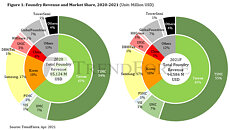
Foundry Revenue Projected to Reach Historical High of US$94.6 Billion in 2021 Thanks to High 5G/HPC/End-Device Demand, Says TrendForce

As the global economy enters the post-pandemic era, technologies including 5G, WiFi6/6E, and HPC (high-performance computing) have been advancing rapidly, in turn bringing about a fundamental, structural change in the semiconductor industry as well, according to TrendForce's latest investigations. While the demand for certain devices such as notebook computers and TVs underwent a sharp uptick due to the onset of the stay-at-home economy, this demand will return to pre-pandemic levels once the pandemic has been brought under control as a result of the global vaccination drive. Nevertheless, the worldwide shift to next-gen telecommunication standards has brought about a replacement demand for telecom and networking devices, and this demand will continue to propel the semiconductor industry, resulting in high capacity utilization rates across the major foundries. As certain foundries continue to expand their production capacities this year, TrendForce expects total foundry revenue to reach a historical high of US$94.6 billion this year, an 11% growth YoY.

China Develops Tools for 28 nm Silicon Manufacturing

When the US decided to impose sanctions on all US-made technology use in foreign countries (China), the Chinese semiconductor manufacturing industry seemed at the time that it would just completely stop. Without the tools to manufacture silicon, Chinese manufacturers would need to turn to other countries to search for a possible solution. That, however, turned out impossible as the US administration has decided to stop the silicon from going into the hands of Chinese companies, by making a condition that any US-made technology can not get to China. Many of the parts for silicon manufacturing are designed in the US, so they have the power to restrict the use.

Today, in a surprising turn of events, we have information that Shanghai Micro Electronic Equipment (SMEE) has developed a deep ultraviolet (DUV) lithography scanner that is set for delivery in 2021. With a plan to deliver it in the fourth quarter of 2021, SMEE has designed this DUV scanner for the production of 28 nm node. While not being the most advanced node available to date, it is a significant start for Chinese technology independence. ASML, the producer of such scanners, used to be one of the few options there, however, it just gained a competitor. China will deliver its new silicon on a 28 nm process at the end of 2021. Pictured below, you can see how the scanner from SMEE looks like.

Intel's 10 nm-Geared Fab 42 Enters Operational Status

Intel has finally sounded the "full steam ahead" whistle for its Fab 42, set in Arizona. Fab 42 has a storied past to it, as Intel started its construction back in 2011. It was actually finished by 2013, and by 2014 all essential infrastructure for semiconductor fabrication was there - except for the fabrication equipment itself. You see, Intel aimed for this factory to produce 450 mm wafers (instead of the industry standard 300 mm) in the 14 nm process. However, back in 2014, Intel wasn't sure about demand for its 14 nm products - and the company was actually planning to debut 10 nm back in 2016, so it sort of made sense. Of course, then came the 10 nm delays, the 14 nm supply issues, and backporting of certain products to other less cutting-edge processes. If only Intel had had a crystal ball.
Return to Keyword Browsing
Jan 17th, 2025 17:54 EST change timezone

New Forum Posts

Popular Reviews

Controversial News Posts