Apr 13th, 2025 15:32 EDT
change timezone
Latest GPU Drivers
New Forum Posts
- should global c-state be "enabled" instead of auto on am5 x3d processors? (25)
- What local LLM-s you use? (154)
- [electronics] - STREAM DECK during gaming? (2)
- Upgrade for a GTX-1060 video card to a X570 AM4 MB w/ a Ryzen 9 3900X (17)
- Dell Latitude 5420 - i7 1185G7 (3)
- Optical Disc Drive owners club (198)
- How to relubricate a fan and/or service a troublesome/noisy fan. (216)
- SK hynix A-Die (Overclocking thread) only for RYZEN AM5 users (30)
- Regarding fan noise (5)
- RX 9000 series GPU Owners Club (309)
Popular Reviews
- Thermaltake TR100 Review
- The Last Of Us Part 2 Performance Benchmark Review - 30 GPUs Compared
- TerraMaster F8 SSD Plus Review - Compact and quiet
- ASUS GeForce RTX 5080 TUF OC Review
- Zotac GeForce RTX 5070 Ti Amp Extreme Review
- ASRock Z890 Taichi OCF Review
- Sapphire Radeon RX 9070 XT Pulse Review
- Sapphire Radeon RX 9070 XT Nitro+ Review - Beating NVIDIA
- Upcoming Hardware Launches 2025 (Updated Apr 2025)
- AMD Ryzen 7 9800X3D Review - The Best Gaming Processor
Controversial News Posts
- NVIDIA GeForce RTX 5060 Ti 16 GB SKU Likely Launching at $499, According to Supply Chain Leak (181)
- MSI Doesn't Plan Radeon RX 9000 Series GPUs, Skips AMD RDNA 4 Generation Entirely (146)
- Microsoft Introduces Copilot for Gaming (124)
- NVIDIA Sends MSRP Numbers to Partners: GeForce RTX 5060 Ti 8 GB at $379, RTX 5060 Ti 16 GB at $429 (123)
- Nintendo Confirms That Switch 2 Joy-Cons Will Not Utilize Hall Effect Stick Technology (105)
- Over 200,000 Sold Radeon RX 9070 and RX 9070 XT GPUs? AMD Says No Number was Given (100)
- Nintendo Switch 2 Launches June 5 at $449.99 with New Hardware and Games (99)
- NVIDIA PhysX and Flow Made Fully Open-Source (77)
News Posts matching #FPGA
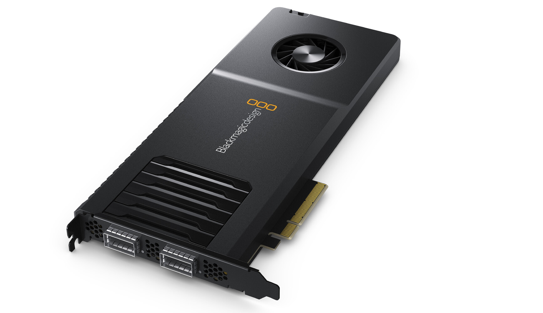
Return to Keyword BrowsingBlackmagic Design Announces New DeckLink IP 100G NIC
Blackmagic Design today announced DeckLink IP 100G, a new PCIe Gen 4 card which can capture and playback up to 8 channels of HD and Ultra HD video simultaneously into 2110 IP systems. It also includes 2 x 100G Ethernet QSFP ports for redundancy, or connecting to two separate 100G Ethernet switches, as well as built in cooling. DeckLink IP 100G also supports GPUDirect RDMA for direct memory transfers between DeckLink and GPUs, reducing PCIe bandwidth when processing video on GPUs for a significant reduction in latency. DeckLink IP 100G will be available in July from Blackmagic Design resellers worldwide for US$1,795.
DeckLink IP 100G will be displayed on the Blackmagic Design NAB 2025 booth #SL216. DeckLink IP cards are the easiest way to capture and play back video directly into 2110 IP based broadcast systems. They have the same DeckLink features so existing software will just work. DeckLink IP cards support multiple video channels plus each channel can capture and play back at the same time. This means customers can build racks of servers generating broadcast graphics, virtual sets or GPU based AI image processing, all directly integrated into 2110 IP broadcast infrastructure. Customers can even use DaVinci Resolve for 2110 IP based broadcast editing workstations. DeckLink IP features a high speed PCIe connection so it works on the latest Mac Pro, Windows and Linux computers.
DeckLink IP 100G will be displayed on the Blackmagic Design NAB 2025 booth #SL216. DeckLink IP cards are the easiest way to capture and play back video directly into 2110 IP based broadcast systems. They have the same DeckLink features so existing software will just work. DeckLink IP cards support multiple video channels plus each channel can capture and play back at the same time. This means customers can build racks of servers generating broadcast graphics, virtual sets or GPU based AI image processing, all directly integrated into 2110 IP broadcast infrastructure. Customers can even use DaVinci Resolve for 2110 IP based broadcast editing workstations. DeckLink IP features a high speed PCIe connection so it works on the latest Mac Pro, Windows and Linux computers.
Altera Starts Production Shipments of Agilex 7 FPGA M-Series
Altera Corporation, a leader in FPGA innovations, today announced production shipments of its Agilex 7 FPGA M-Series, the industry's first high-end, high-density FPGA to feature integrated high bandwidth memory and support for DDR5 and LPDDR5 memory technologies. Offering over 3.8 million logic elements, Agilex 7 FPGA M-Series is optimized for applications that demand the highest performance and highest memory bandwidth, including AI, data centers, next-generation firewalls, 5G communications infrastructure and 8K broadcast equipment.
As data traffic continues to increase exponentially due to the growth of AI, cloud computing and video streaming services, the demand for higher memory bandwidth, increased capacity, and improved power efficiency has never been greater. Agilex 7 FPGA M-Series addresses these challenges by offering users high logic densities, a high-performance fabric and a memory interface that accelerates data throughput speeds while reducing memory bottlenecks and latency.
As data traffic continues to increase exponentially due to the growth of AI, cloud computing and video streaming services, the demand for higher memory bandwidth, increased capacity, and improved power efficiency has never been greater. Agilex 7 FPGA M-Series addresses these challenges by offering users high logic densities, a high-performance fabric and a memory interface that accelerates data throughput speeds while reducing memory bottlenecks and latency.

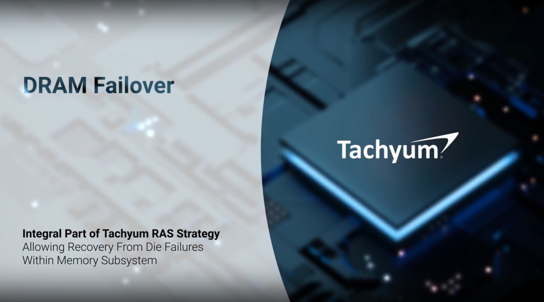
Tachyum Demonstrates DRAM Failover for Large Scale AI on Prodigy FPGA Prototype
Tachyum today announced that it has successfully enabled DRAM Failover correct system on its Prodigy Universal Processor, demonstrating enhanced reliability for even larger-scale AI and HPC applications even in the case of DRAM chip failures.
Tachyum's DRAM Failover is an advanced memory error correction technology that improves the reliability of DRAM and provides a higher level of protection than traditional Error Correction Code (ECC). DRAM Failover can correct multi-bit errors within a single memory chip or across multiple memory chips, allowing continued memory operation in the event of device-level faults in memory. With DRAM Failover, even a whole DRAM chip failure can be tolerated without affecting the system and applications.
Tachyum's DRAM Failover is an advanced memory error correction technology that improves the reliability of DRAM and provides a higher level of protection than traditional Error Correction Code (ECC). DRAM Failover can correct multi-bit errors within a single memory chip or across multiple memory chips, allowing continued memory operation in the event of device-level faults in memory. With DRAM Failover, even a whole DRAM chip failure can be tolerated without affecting the system and applications.
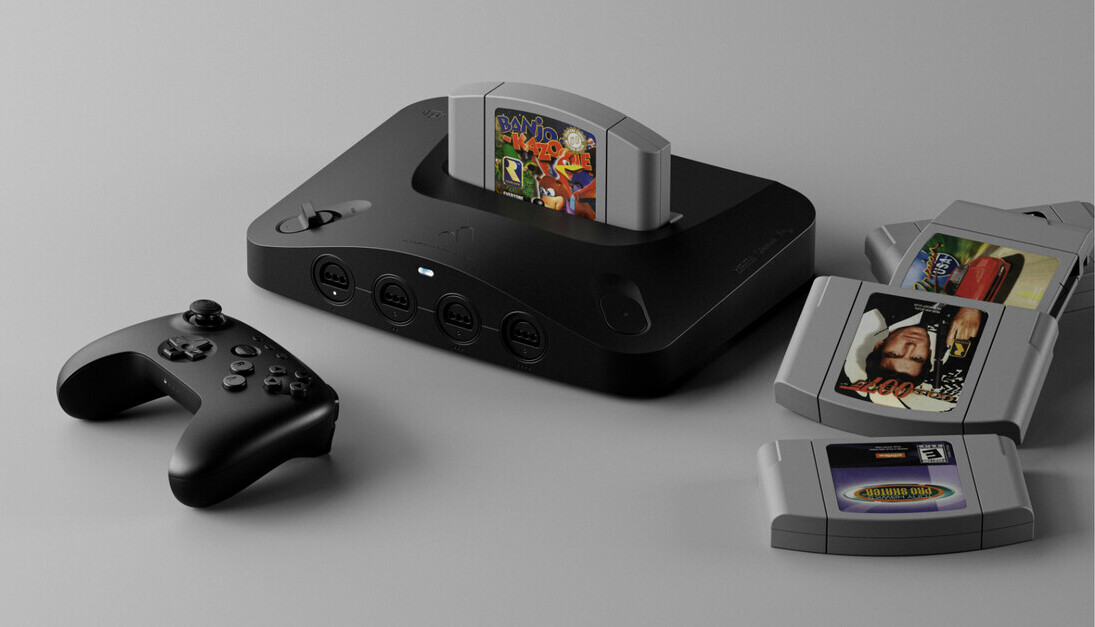
Analogue 3D Launch Window Pushed into July, FPGA-powered Console Previously Delayed into Q1
Analogue's modern reimagining of Nintendo's N64 home console has hit another pre-release obstacle. Their Analogue 3D model was first revealed in 2023, with a projected 2024 launch on the cards. The system has experienced a series of setbacks—prior to the latest official announcement, customers were expecting to receive finalized hardware by now (first quarter of 2025). Once again, the company has revised release timeframes for its $249.99 FPGA-powered console—according to an official "3D Preorder FAQ": "Analogue 3D was originally available for pre-order at the end of 2024, (and) scheduled to ship Q1 2025. Shipping is delayed (as of March 18th, 2025) and is now shipping by July 2025. We are working hard to get your 3D order in hands ASAP, and appreciate your patience. If you have an open pre-order no action is needed. As always, if you'd like to cancel your pre-order at any time, Analogue has always had a no questions asked, 100% refund policy for pre-orders."
Analogue's promotional materials showcase a very slick-looking premium reinterpretation (in black or white) of the classic N64 system. The R&D team spent: "nearly four years engineering it in FPGA. No more incompatibilities found in software emulation like input lag, graphic/audio inaccuracies, timing/frame rate issues and more. For the first time, you can re-experience the N64 exactly as it was meant to be, without compromise." According to product pages, a controller is not bundled in with the Analogue 3D package. Authentic front panel connectors indicate customers having to reuse original "trident-shaped" N64 (NUS-005) controllers, or third-party equivalents. Certain promo shots show off 8BitDo's recently introduced 64 Bluetooth Controller. Given Analogue's revised schedule, this wireless gamepad is expected to arrive weeks ahead of its natural partner piece.


Analogue's promotional materials showcase a very slick-looking premium reinterpretation (in black or white) of the classic N64 system. The R&D team spent: "nearly four years engineering it in FPGA. No more incompatibilities found in software emulation like input lag, graphic/audio inaccuracies, timing/frame rate issues and more. For the first time, you can re-experience the N64 exactly as it was meant to be, without compromise." According to product pages, a controller is not bundled in with the Analogue 3D package. Authentic front panel connectors indicate customers having to reuse original "trident-shaped" N64 (NUS-005) controllers, or third-party equivalents. Certain promo shots show off 8BitDo's recently introduced 64 Bluetooth Controller. Given Analogue's revised schedule, this wireless gamepad is expected to arrive weeks ahead of its natural partner piece.


Altera Begins Shipping Agilex 3 AI FPGAs
Today at Embedded World, Altera Corporation, a leader in FPGA innovations, unveiled its latest programmable solutions tailored for embedded developers who are pushing the boundaries of innovation at the intelligent edge. Altera's latest Agilex FPGAs, Quartus Prime Pro software, and FPGA AI Suite enable the rapid development of highly customized embedded systems deployed across a broad range of edge applications, including robotics, factory automation systems, and medical equipment.
Altera's programmable solutions meet the stringent power, performance and size requirements of embedded and intelligent edge applications. These hardware solutions, along with Altera's FPGA AI Suite, enable machine learning engineers, software developers, and FPGA designers to create custom FPGA AI platforms using industry-standard frameworks such as TensorFlow and PyTorch, and development tools such as OpenVINO and Quartus Prime software.
Altera's programmable solutions meet the stringent power, performance and size requirements of embedded and intelligent edge applications. These hardware solutions, along with Altera's FPGA AI Suite, enable machine learning engineers, software developers, and FPGA designers to create custom FPGA AI platforms using industry-standard frameworks such as TensorFlow and PyTorch, and development tools such as OpenVINO and Quartus Prime software.

Logic Fruit Technologies Releases High-Speed Interface IPs Stack for Advanced Computing
Logic Fruit Technologies, a leading provider of cutting-edge FPGA-based solutions, proudly announces the release of its latest High-Speed Interface IP stack, including PCIe Gen 6 Controller IP, PCIe Gen 6 PHY IP, and CXL 3 Controller IP.
These high-performance solutions enable seamless data transfer, ensuring reliability, scalability, and efficiency for next-generation computing applications such as AI/ML, data centers, and high-performance networking.
These high-performance solutions enable seamless data transfer, ensuring reliability, scalability, and efficiency for next-generation computing applications such as AI/ML, data centers, and high-performance networking.


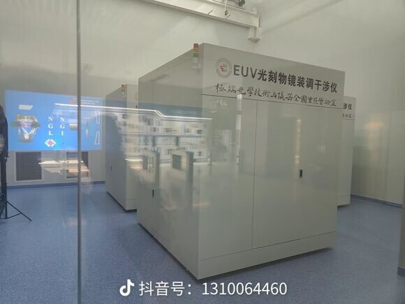
China Develops Domestic EUV Tool, ASML Monopoly in Trouble
China's domestic extreme ultraviolet (EUV) lithography development is far from a distant dream. The newest system, now undergoing testing at Huawei's Dongguan facility, leverages laser-induced discharge plasma (LDP) technology, representing a potentially disruptive approach to EUV light generation. The system is scheduled for trial production in Q3 2025, with mass manufacturing targeted for 2026, potentially positioning China to break ASML's technical monopoly in advanced lithography. The LDP approach employed in the Chinese system generates 13.5 nm EUV radiation by vaporizing tin between electrodes and converting it to plasma via high-voltage discharge, where electron-ion collisions produce the required wavelength. This methodology offers several technical advantages over ASML's laser-produced plasma (LPP) technique, including simplified architecture, reduced footprint, improved energy efficiency, and potentially lower production costs.
The LPP method relies on high-energy lasers and complex FPGA-based real-time control electronics to achieve the same result. While ASML has refined its LPP-based systems over decades, the inherent efficiency advantages of the LDP approach could accelerate China's catch-up timeline in this critical semiconductor manufacturing technology. When the US imposed sanctions on EUV shipments to Chinese companies, the Chinese semiconductor development was basically limited as standard deep ultraviolet (DUV) wave lithography systems utilize 248 nm (KrF) and 193 nm (ArF) wavelengths for semiconductor patterning, with 193 nm immersion technology representing the most advanced pre-EUV production technique. These longer wavelengths contrast with EUV's 13.5 nm radiation, requiring multiple patterning techniques to achieve advanced nodes.

The LPP method relies on high-energy lasers and complex FPGA-based real-time control electronics to achieve the same result. While ASML has refined its LPP-based systems over decades, the inherent efficiency advantages of the LDP approach could accelerate China's catch-up timeline in this critical semiconductor manufacturing technology. When the US imposed sanctions on EUV shipments to Chinese companies, the Chinese semiconductor development was basically limited as standard deep ultraviolet (DUV) wave lithography systems utilize 248 nm (KrF) and 193 nm (ArF) wavelengths for semiconductor patterning, with 193 nm immersion technology representing the most advanced pre-EUV production technique. These longer wavelengths contrast with EUV's 13.5 nm radiation, requiring multiple patterning techniques to achieve advanced nodes.

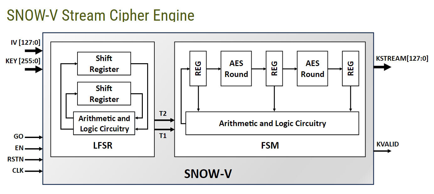
CAST Releases First Commercial SNOW-V Stream Cipher IP Core
Semiconductor intellectual property core provider CAST today announced a new IP core that implements the SNOW-V stream cipher algorithm to meet the security and performance demands of modern communication systems. Available now for ASICs or FPGAs, the company believes it to be the first such commercial IP core.
The new SNOW-V Stream Cipher Engine provides a flexible and reusable hardware implementation of the official SNOW-V mechanism as published in 2019 by the IACR Transactions on Symmetric Cryptology. SNOW-V revises the SNOW 3G stream cipher algorithm to help satisfy the high-speed, low-latency security requirements of 5G, 6G, and future mobile networks. The core:
The new SNOW-V Stream Cipher Engine provides a flexible and reusable hardware implementation of the official SNOW-V mechanism as published in 2019 by the IACR Transactions on Symmetric Cryptology. SNOW-V revises the SNOW 3G stream cipher algorithm to help satisfy the high-speed, low-latency security requirements of 5G, 6G, and future mobile networks. The core:
Synopsys Expands Its Hardware-Assisted Verification (HAV) Portfolio for Next-Gen Semiconductors
Synopsys, Inc. today announced the expansion of its industry-leading hardware-assisted verification (HAV) portfolio with new HAPS prototyping and ZeBu emulation systems using the latest AMD Versal Premium VP1902 adaptive SoC. The next generation HAPS-200 prototyping and ZeBu-200 emulation systems deliver improved runtime performance, better compile time and improved debug productivity. They are built on new Synopsys Emulation and Prototyping (EP-Ready) Hardware that optimizes customer return on investment by enabling emulation and prototyping use cases via reconfiguration and optimized software. ZeBu Server 5 is enhanced to deliver industry-leading scalability beyond 60 billion gates (BG) to address the escalating hardware and software complexity in SoC and multi-die designs. It continues to offer industry-best density to optimize data center space utilization.
"With the industry approaching 100s of billions of gates per chip and 100s of millions of lines of software code in SoC and multi-die solutions, verification of advanced designs poses never-before seen challenges," said Ravi Subramanian, chief product management officer, Synopsys. "Continuing our strong partnership with AMD, our new systems deliver the highest HAV performance while offering the ultimate flexibility between prototyping and emulation use. Industry leaders are adopting Synopsys EP-Ready Hardware platforms for silicon to system verification and validation."

"With the industry approaching 100s of billions of gates per chip and 100s of millions of lines of software code in SoC and multi-die solutions, verification of advanced designs poses never-before seen challenges," said Ravi Subramanian, chief product management officer, Synopsys. "Continuing our strong partnership with AMD, our new systems deliver the highest HAV performance while offering the ultimate flexibility between prototyping and emulation use. Industry leaders are adopting Synopsys EP-Ready Hardware platforms for silicon to system verification and validation."


Artificial Intelligence (AI) Chips Market to Grow by USD 902.6 Billion by 2029: Technavio
Report with market evolution powered by AI—The global artificial intelligence (AI) chips market size is estimated to grow by USD 902.6 billion from 2025-2029, according to Technavio. The market is estimated to grow at a CAGR of over 81.2% during the forecast period. Increased focus on developing AI chips for smartphones is driving market growth, with a trend towards convergence of AI and IoT. However, dearth of technically skilled workers for ai chips development poses a challenge. Key market players include Advanced Micro Devices Inc., Baidu Inc., Broadcom Inc., Cerebras, Fujitsu Ltd., Google LLC, Graphcore Ltd., Huawei Technologies Co. Ltd., Intel Corp., International Business Machines Corp., MediaTek Inc., Microchip Technology Inc., NVIDIA Corp., NXP Semiconductors NV, Qualcomm Inc., SambaNova Systems Inc., Samsung Electronics Co. Ltd., SenseTime Group Inc., Taiwan Semiconductor Manufacturing Co. Ltd., and Tesla Inc.


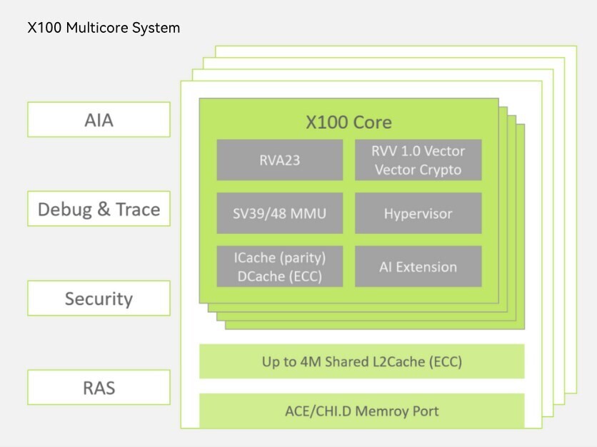
RISC-V Breakthrough: SpacemiT Develops Server CPU Chip V100 for Next-Gen AI Applications
Recently, SpacemiT, a RISC-V AI CPU company from China, announced breakthrough progress in the development of its server CPU chip SpacemiT Vital Stone V100. It now provides a complete RISC-V CPU chip hardware and software platform that fully supports server specifications.
RISC-V CPU core X100, AIA and APLIC supporting interrupt virtualization, IOMMU supporting memory virtualization, IOPMP supporting security functions, LPC and eSPI supporting communication with mainstream BMCs, etc.

RISC-V CPU core X100, AIA and APLIC supporting interrupt virtualization, IOMMU supporting memory virtualization, IOPMP supporting security functions, LPC and eSPI supporting communication with mainstream BMCs, etc.
- The 64-bit server-grade RISC-V CPU core X100 delivers a single-core performance of >9 points/GHz on SPECINT2006 at 2.5 GHz 12 nm. X100 supports the RVA23 Profile, full virtualization (Hypervisor 1.0, AIA 1.0, IOMMU), RAS features, Vector 1.0 extension, vector encryption and decryption, security, 64-core interconnect, and more.
- The IOMMU IP adheres to the RISC-V IOMMU architecture specification and the AXI4-Stream DTI interface, supporting configurable DID, PID, virtual address, physical address width, and various levels of translation cache sizes. It can be flexibly integrated into different locations within the SoC bus system to enable distributed peripheral virtualization and accelerator acceleration.

Lattice Advances Low Power FPGA Leadership with New Small and Mid-range FPGA Offerings
Today, at Lattice Developers Conference 2024, Lattice Semiconductor expanded its edge to cloud FPGA innovation leadership with the launch of exciting new hardware and software solutions. The new Lattice Nexus 2 next-gen small FPGA platform and the first device family based on the platform, Lattice Certus -N2 general purpose FPGAs, offer advanced connectivity, optimized power and performance, and class-leading security. Lattice also announced new mid-range FPGA device capacity options - Lattice Avant 30 and Avant 50 - and new versions of Lattice design software tools and application-specific solution stacks to help accelerate customer time-to-market.
"At Lattice, we are proud to lead technological advancements in low power, small form factor FPGAs, ensuring our customers have the optimal devices, tools, and solutions to design groundbreaking applications that are power efficient, fast, and secure," said Esam Elashmawi, Chief Strategy and Marketing Officer, Lattice Semiconductor. "From the edge to the cloud across a variety of industries, FPGAs stand at the forefront of innovation, and we're committed to delivering versatile and robust small and mid-range FPGA solutions that enable our customers and partners to unlock their full potential."
"At Lattice, we are proud to lead technological advancements in low power, small form factor FPGAs, ensuring our customers have the optimal devices, tools, and solutions to design groundbreaking applications that are power efficient, fast, and secure," said Esam Elashmawi, Chief Strategy and Marketing Officer, Lattice Semiconductor. "From the edge to the cloud across a variety of industries, FPGAs stand at the forefront of innovation, and we're committed to delivering versatile and robust small and mid-range FPGA solutions that enable our customers and partners to unlock their full potential."


AMD Introduces Versal RF Series Adaptive SoCs With Integrated Direct RF-Sampling Converters
AMD today announced the expansion of the AMD Versal adaptive system-on-chip (SoC) portfolio with the introduction of the Versal RF Series that includes the industry's highest compute performance in a single-chip device with integrated direct radio frequency (RF)-sampling data converters.
Versal RF Series offers precise, wideband-spectrum observability and up to 80 TOPS of digital signal processing (DSP) performance in a size, weight, and power (SWaP)-optimized design, targeting RF systems and test equipment applications in the aerospace and defense (A&D) and test and measurement (T&M) markets, respectively.

Versal RF Series offers precise, wideband-spectrum observability and up to 80 TOPS of digital signal processing (DSP) performance in a size, weight, and power (SWaP)-optimized design, targeting RF systems and test equipment applications in the aerospace and defense (A&D) and test and measurement (T&M) markets, respectively.


Lattice Semiconductor Explores Buying Intel's Altera Unit
Intel Altera's FPGA unit is attracting a lot of attention in the semiconductor industry according to a recent report by Bloomberg, Lattice Semiconductor emerging as a potential buyer for the entire division. Bloomberg reports that Lattice actively works with advisers and seeks private-sector backing to support their bid. However, Intel's preference appears to be leaning toward selling only a small portion of its Altera shares instead of selling everything and this can be a decisive factor in upcoming negotiations. The potential sale has attracted interest from many outside Lattice Semiconductor, including major private equity firms such as Francisco Partners, Bain Capital, and Silver Lake Management. Qualcomm has also expressed interest in acquiring parts of Intel's design business.
Bloomberg also reports that selling just a portion of Altera's shares would likely require complex financial arrangements, while private equity firms are considering investing about $3 billion through instruments. This could result in Intel's valuation being lower than the original purchase price. Intel CEO Pat Gelsinger has indicated plans to close the Altera transaction in early 2024, with the company valuing the nearly $16.7 billion Intel paid for Altera in 2015 at approximately $17 billion. Lattice's market value of $7.48 billion is certainly smaller and can challenge Lattice's ambitions for complete control of Altera. The Intel board discussed Altera's future last week and prefers to sell only a minority stake, with a decision expected soon.
Bloomberg also reports that selling just a portion of Altera's shares would likely require complex financial arrangements, while private equity firms are considering investing about $3 billion through instruments. This could result in Intel's valuation being lower than the original purchase price. Intel CEO Pat Gelsinger has indicated plans to close the Altera transaction in early 2024, with the company valuing the nearly $16.7 billion Intel paid for Altera in 2015 at approximately $17 billion. Lattice's market value of $7.48 billion is certainly smaller and can challenge Lattice's ambitions for complete control of Altera. The Intel board discussed Altera's future last week and prefers to sell only a minority stake, with a decision expected soon.

Ubitium Debuts First Universal RISC-V Processor: CPU, GPU, DSP, FPGA All in One Chip
For over half a century, general-purpose processors have been built on the Tomasulo algorithm, developed by IBM engineer Robert Tomasulo in 1967. It's a $500B industry built on specialized CPU, GPU and other chips for different computing tasks. Hardware startup Ubitium has shattered this paradigm with a breakthrough universal processor that handles all computing workloads on a single, efficient chip - unlocking simpler, smarter, and more cost-effective devices across industries - while revolutionizing a 57-year-old industry standard.
Alongside this, Ubitium is announcing a $3.7 million in seed funding round, co-led by Runa Capital, Inflection, and KBC Focus Fund. The investment will be used to develop the first prototypes and prepare initial development kits for customers, with the first chips planned for 2026.
Alongside this, Ubitium is announcing a $3.7 million in seed funding round, co-led by Runa Capital, Inflection, and KBC Focus Fund. The investment will be used to develop the first prototypes and prepare initial development kits for customers, with the first chips planned for 2026.

AMD Unveils the Versal Premium Series Gen 2 Adaptive SoC (FPGA) with PCIe 6.0 and CXL 3.1 For Next-Gen, I/O Rich Applications
AMD on Tuesday released its flagship FPGA series, and possibly its most important product launch after the company's Xilinx acquisition, the Versal Premium Series Gen 2 SoC. It's hard to call this an FPGA, much in the same way as it's hard to call a modern processor "a CPU," there are many integrated devices, platform interfaces, and application-specific accelerators, and much in the same way, the Versal Premium Series Gen 2 is marketed as an "adaptive SoC," rather than a really powerful FPGA. Speaking of I/O, this is AMD's first product to implement PCI-Express Gen 6 and CXL 3.1.
There's no host platform that currently support these standards—neither EPYC "Turin" nor Xeon 6 "Granite Rapids," but it goes to show that the chip is future-ready and can put the new I/O standards to use. The chip is designed to be implemented as a standalone SoC, and so it supports both DDR5 RDIMMs and LPDDR5X, giving end-users the flexibility to go with the two vastly different memory standards depending on what their application is. These capabilities make the Versal Premium Series Gen 2 well-suited for demanding applications in sectors like data centers, communications, test and measurement, aerospace, and defense, where high-speed data processing is critical.


There's no host platform that currently support these standards—neither EPYC "Turin" nor Xeon 6 "Granite Rapids," but it goes to show that the chip is future-ready and can put the new I/O standards to use. The chip is designed to be implemented as a standalone SoC, and so it supports both DDR5 RDIMMs and LPDDR5X, giving end-users the flexibility to go with the two vastly different memory standards depending on what their application is. These capabilities make the Versal Premium Series Gen 2 well-suited for demanding applications in sectors like data centers, communications, test and measurement, aerospace, and defense, where high-speed data processing is critical.


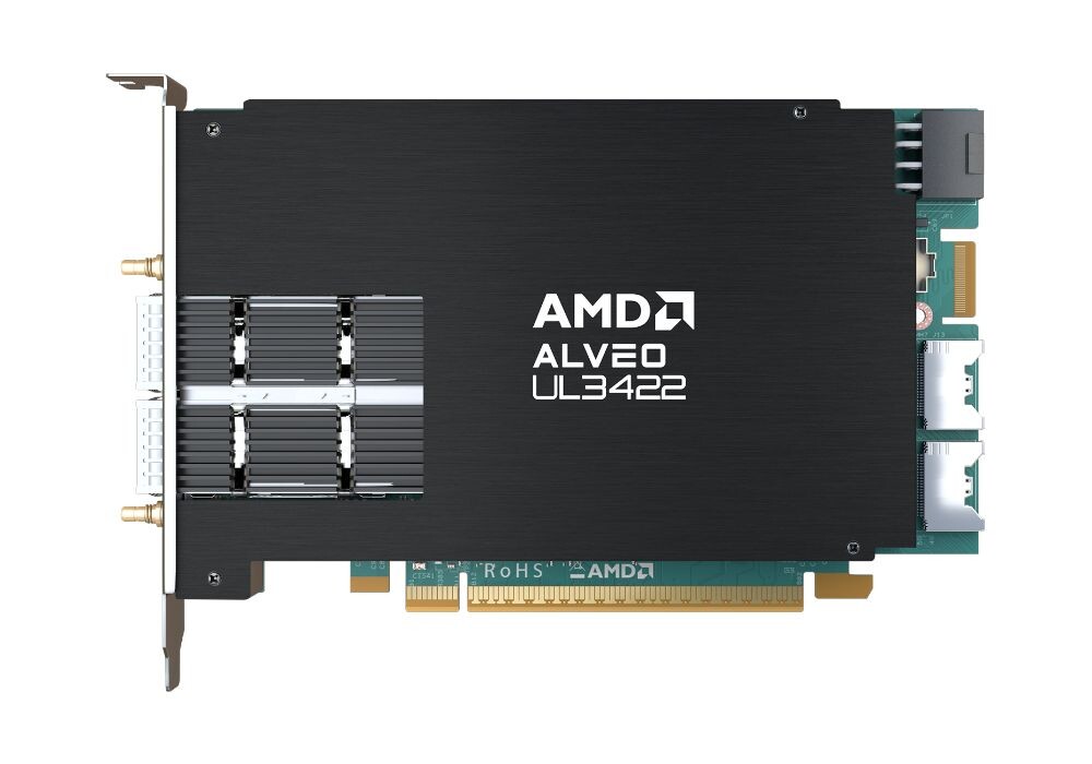
AMD Launches New Slim Form Factor Alveo UL3422 Accelerator Card
AMD today announced the AMD Alveo UL3422 accelerator card, the latest addition to its record-breaking family of accelerators1 designed for ultra-low latency electronic trading applications. AMD Alveo UL3422 provides trading firms, market makers and financial institutions with a slim form factor accelerator optimized for rack space, cost and designed for a fast path to deployment in a wide range of servers. The Alveo UL3422 accelerator is powered by an AMD Virtex UltraScale+ FPGA that features a novel transceiver architecture with hardened, optimized network connectivity cores, custom built for high-speed trading. It enables ultra-low latency trade execution, achieving less than 3ns FPGA transceiver latency and breakthrough 'tick-to-trade' performance not achievable with standard off-the-shelf FPGAs.
"Speed is the ultimate advantage in the increasingly competitive world of high-speed trading," said Yousef Khalilollahi, corporate vice president & general manager, Adaptive Computing Group, AMD. "The Alveo UL3422 card provides a lower-cost entry point while still delivering cutting-edge latency performance, making it accessible to firms of all sizes that want to stay competitive in the ultra-low latency trading space."
"Speed is the ultimate advantage in the increasingly competitive world of high-speed trading," said Yousef Khalilollahi, corporate vice president & general manager, Adaptive Computing Group, AMD. "The Alveo UL3422 card provides a lower-cost entry point while still delivering cutting-edge latency performance, making it accessible to firms of all sizes that want to stay competitive in the ultra-low latency trading space."
Jabil Intros New Servers Powered by AMD 5th Gen EPYC and Intel Xeon 6 Processors
Jabil Inc. announced today that it is expanding its server portfolio with the J421E-S and J422-S servers, powered by AMD 5th Generation EPYC and Intel Xeon 6 processors. These servers are purpose-built for scalability in a variety of cloud data center applications, including AI, high-performance computing (HPC), fintech, networking, storage, databases, and security — representing the latest generation of server innovation from Jabil.
Built with customization and innovation in mind, the design-ready J422-S and J421E-S servers will allow engineering teams to meet customers' specific requirements. By fine-tuning Jabil's custom BIOS and BMC firmware, Jabil can create a competitive advantage for customers by developing the server configuration needed for higher performance, data management, and security. The server platforms are now available for sampling and will be in production by the first half of 2025.

Built with customization and innovation in mind, the design-ready J422-S and J421E-S servers will allow engineering teams to meet customers' specific requirements. By fine-tuning Jabil's custom BIOS and BMC firmware, Jabil can create a competitive advantage for customers by developing the server configuration needed for higher performance, data management, and security. The server platforms are now available for sampling and will be in production by the first half of 2025.


Infineon Introduces the Industry's First 20 Gbps Universal USB Peripheral Controller
Infineon Technologies AG today announced the addition of the EZ-USB FX20 programmable USB peripheral controller to its EZ-USB product family. It enables developers to create USB devices that meet the highest performance requirements in AI, image processing and emerging applications. The EZ-USB FX20 peripheral controller offers high-speed connectivity with USB 20 Gbps and LVDS interfaces, increasing the total bandwidth up to six times over its predecessor, the EZ-USB FX3.
"With the growing popularity of USB devices, the demand for compatible and adaptable USB controllers is increasing," said Ganesh Subramaniam, Senior Vice President and General Manager of the Wired Connectivity Solutions Product Line at Infineon. "Therefore, we are continuously improving the features and performance of our EZ-USB peripheral controllers and are pleased to support developers with our new addition to the product family, providing them with a flexible component to create powerful and advanced applications."

"With the growing popularity of USB devices, the demand for compatible and adaptable USB controllers is increasing," said Ganesh Subramaniam, Senior Vice President and General Manager of the Wired Connectivity Solutions Product Line at Infineon. "Therefore, we are continuously improving the features and performance of our EZ-USB peripheral controllers and are pleased to support developers with our new addition to the product family, providing them with a flexible component to create powerful and advanced applications."


Altera Announces Agilex 3 Series FPGAs and Agilex 5 Development Kits
Altera, an Intel Company, today unveiled an array of FPGA hardware, software and development tools that make its programmable solutions more accessible across a broader range of use cases and markets. At its annual developer's conference, Altera revealed new details on its next-generation, power- and cost-optimized Agilex 3 FPGAs and announced new development kits and software support for its Agilex 5 FPGAs.
"Working closely with our ecosystem and distribution partners, Altera remains committed to delivering FPGA-based solutions that empower innovators with leading-edge programmable technologies that are easy to design and deploy. With these key announcements, we continue to execute on our vision of shaping the future by using programmable logic to help customers unlock greater value across a broad range of use cases within the data center, aerospace and defense sectors, communications infrastructure, automotive, industrial, test, medical and embedded markets," said Sandra Rivera, CEO of Altera.
"Working closely with our ecosystem and distribution partners, Altera remains committed to delivering FPGA-based solutions that empower innovators with leading-edge programmable technologies that are easy to design and deploy. With these key announcements, we continue to execute on our vision of shaping the future by using programmable logic to help customers unlock greater value across a broad range of use cases within the data center, aerospace and defense sectors, communications infrastructure, automotive, industrial, test, medical and embedded markets," said Sandra Rivera, CEO of Altera.

Magewell Expands Renowned USB Capture Product Family with New 4K/60fps Model
Magewell's USB Capture family has long been the gold standard for professional video capture devices, earning a reputation for being the easiest and most reliable way to bring video and audio signals into software for live streaming, video conferencing, medical imaging and more. Magewell has expanded the renowned product line with the unveiling of a new model that captures video sources up to 4K resolution at 60 frames per second - the USB Capture HDMI 4K Pro. The new model will be demonstrated alongside other Magewell innovations in stand 7.A44 at the IBC2024 exhibition in Amsterdam from September 13 to 16.
Magewell's compact USB Capture devices enable computers including laptops to capture high-quality AV signals through a USB interface, with no additional power source required. The new USB Capture HDMI 4K Pro offers everything that users love about the existing USB Capture HDMI 4K Plus model, while leveraging 20 Gbps USB transfer performance on compatible host systems to enable the capture of 4K video at higher frame rates and color precision.


Magewell's compact USB Capture devices enable computers including laptops to capture high-quality AV signals through a USB interface, with no additional power source required. The new USB Capture HDMI 4K Pro offers everything that users love about the existing USB Capture HDMI 4K Plus model, while leveraging 20 Gbps USB transfer performance on compatible host systems to enable the capture of 4K video at higher frame rates and color precision.


Intel Considers Sale of Altera Business Amid Restructuring Plans, Foundry Business to Stay
Intel is reportedly exploring the sale of its Altera business, a move guided by CEO Pat Gelsinger as part of broader restructuring efforts. Acquired by Intel in 2015 for $16.7 billion, Altera, formerly known as the Programmable Solutions Group, has been a profitable segment. However, with Intel facing financial strain due to extensive spending, the company is now considering divesting its FPGA business to recoup capital. Currently, Altera operates as a separate entity within Intel, relying on the tech giant for R&D, sales, marketing, and support. Gelsinger is expected to propose the sale at a board meeting scheduled for mid-September, where he will outline his vision for Intel's future. This restructuring could also affect other parts of Intel's operations, including its Foundry business.
While previous reports suggested that Intel might spin off its Foundry unit or sell it to industry leaders like TSMC or Samsung, the latest information indicates that Intel plans to retain this division, albeit with scaled-back expansion efforts. The $32 billion factory in Germany, for example, may be scrapped, along with other capital-intensive projects, and other capital expansions may also be put on hold. Pat Gelsinger's vision still needs to be finalized and is still in the drafting phase, so until the mid-September board meeting, we have to wait to gain more information.
While previous reports suggested that Intel might spin off its Foundry unit or sell it to industry leaders like TSMC or Samsung, the latest information indicates that Intel plans to retain this division, albeit with scaled-back expansion efforts. The $32 billion factory in Germany, for example, may be scrapped, along with other capital-intensive projects, and other capital expansions may also be put on hold. Pat Gelsinger's vision still needs to be finalized and is still in the drafting phase, so until the mid-September board meeting, we have to wait to gain more information.

Tachyum Builds Last FPGA Prototypes Batch Ahead of Tape-Out
Tachyum today announced the final build of its Prodigy FPGA emulation system in advance of chip production and general availability next year. As part of the announcement, the company is also ending its purchase program for prototype systems that was previously offered to commercial and federal customers.
These last hardware FPGA prototype units will ensure Tachyum hits its extreme-reliability test targets of more than 10 quadrillion cycles prior to tape-out and before the first Prodigy chips hit the market. Tachyum's software emulation system - and access to it - is expanding with additional availability of open-source software ported ahead of Prodigy's upstreaming.
These last hardware FPGA prototype units will ensure Tachyum hits its extreme-reliability test targets of more than 10 quadrillion cycles prior to tape-out and before the first Prodigy chips hit the market. Tachyum's software emulation system - and access to it - is expanding with additional availability of open-source software ported ahead of Prodigy's upstreaming.
Intel to Cut 10,000 Jobs Across the Globe, Projected to Save $10 Billion
According to sources close to Bloomberg, Intel plans to cut 10,000 jobs from its global workforce. The news comes amid heavy pressure on the semiconductor giant, which has been on a steady decline over the years, while other industry rivals like AMD and NVIDIA have been rising and taking market share in various areas from Intel. It is reported that Intel currently has 110,000 employees globally, and reducing the workforce by 10,000 would net Intel around 100,000 global employees left. These figures exclude employees from spun-out units like Altera FPGA company, which is under Intel's ownership. Intel's aim to reduce its workforce is expected to come with a significant cost benefit to the company, with projected savings of $10 billion by 2025.
The news isn't yet official, but it is expected to see the light of the day as soon as this week. As Intel's CEO Pat Gelsinger invests heavily into the fab construction and development of next-generation products, there have been a few notes that Intel would have to overcome some challenges shortly to reach its long-term goals like more advanced silicon manufacturing facilities and new products for AI/HPC and client sector. One of those short-term measures is reducing the workforce to cut down expenses. Intel has reduced its workforce before. In 2022, the company announced reduced spending in non-critical areas and reducing the workforce, and in 2023, cut the workforce by 5% to 124,800 employees last year, only to be left with 110,000 employees in 2024.
The news isn't yet official, but it is expected to see the light of the day as soon as this week. As Intel's CEO Pat Gelsinger invests heavily into the fab construction and development of next-generation products, there have been a few notes that Intel would have to overcome some challenges shortly to reach its long-term goals like more advanced silicon manufacturing facilities and new products for AI/HPC and client sector. One of those short-term measures is reducing the workforce to cut down expenses. Intel has reduced its workforce before. In 2022, the company announced reduced spending in non-critical areas and reducing the workforce, and in 2023, cut the workforce by 5% to 124,800 employees last year, only to be left with 110,000 employees in 2024.

MaxLinear to Showcase Panther III at Future of Memory and Storage 2024 Trade Show
MaxLinear, Inc., a leading provider of data storage acceleration solutions for enterprise and data center applications, today announced it will demonstrate the advanced compression, encryption, and security performance of its storage acceleration solution, Panther III, at the Future of Memory and Storage (FMS) 2024 trade show from August 6-8, 2024. The demos will show that Panther III can achieve up to 40 times more throughput, up to 190 times better latency, and up to 1000 times less CPU utilization than a software-only solution, leading to significant cost savings in terms of flash drives and needed CPU cores.
MaxLinear's Panther III creates a bold new product category for maximizing the performance of data storage systems - a comprehensive, all-in-one "storage accelerator." Unlike encryption and/or compression solutions, MaxLinear's Panther III consolidates a comprehensive suite of storage acceleration functions, including compression, deduplication, encryption, data protection, and real-time validation, in a single hardware-based solution. Panther III is engineered to offload and expedite specific data processing tasks, thus providing a significant performance boost, storage cost savings, and energy savings compared to traditional software-only, FPGA, and other competitive solutions.
MaxLinear's Panther III creates a bold new product category for maximizing the performance of data storage systems - a comprehensive, all-in-one "storage accelerator." Unlike encryption and/or compression solutions, MaxLinear's Panther III consolidates a comprehensive suite of storage acceleration functions, including compression, deduplication, encryption, data protection, and real-time validation, in a single hardware-based solution. Panther III is engineered to offload and expedite specific data processing tasks, thus providing a significant performance boost, storage cost savings, and energy savings compared to traditional software-only, FPGA, and other competitive solutions.

Apr 13th, 2025 15:32 EDT
change timezone
Latest GPU Drivers
New Forum Posts
- should global c-state be "enabled" instead of auto on am5 x3d processors? (25)
- What local LLM-s you use? (154)
- [electronics] - STREAM DECK during gaming? (2)
- Upgrade for a GTX-1060 video card to a X570 AM4 MB w/ a Ryzen 9 3900X (17)
- Dell Latitude 5420 - i7 1185G7 (3)
- Optical Disc Drive owners club (198)
- How to relubricate a fan and/or service a troublesome/noisy fan. (216)
- SK hynix A-Die (Overclocking thread) only for RYZEN AM5 users (30)
- Regarding fan noise (5)
- RX 9000 series GPU Owners Club (309)
Popular Reviews
- Thermaltake TR100 Review
- The Last Of Us Part 2 Performance Benchmark Review - 30 GPUs Compared
- TerraMaster F8 SSD Plus Review - Compact and quiet
- ASUS GeForce RTX 5080 TUF OC Review
- Zotac GeForce RTX 5070 Ti Amp Extreme Review
- ASRock Z890 Taichi OCF Review
- Sapphire Radeon RX 9070 XT Pulse Review
- Sapphire Radeon RX 9070 XT Nitro+ Review - Beating NVIDIA
- Upcoming Hardware Launches 2025 (Updated Apr 2025)
- AMD Ryzen 7 9800X3D Review - The Best Gaming Processor
Controversial News Posts
- NVIDIA GeForce RTX 5060 Ti 16 GB SKU Likely Launching at $499, According to Supply Chain Leak (181)
- MSI Doesn't Plan Radeon RX 9000 Series GPUs, Skips AMD RDNA 4 Generation Entirely (146)
- Microsoft Introduces Copilot for Gaming (124)
- NVIDIA Sends MSRP Numbers to Partners: GeForce RTX 5060 Ti 8 GB at $379, RTX 5060 Ti 16 GB at $429 (123)
- Nintendo Confirms That Switch 2 Joy-Cons Will Not Utilize Hall Effect Stick Technology (105)
- Over 200,000 Sold Radeon RX 9070 and RX 9070 XT GPUs? AMD Says No Number was Given (100)
- Nintendo Switch 2 Launches June 5 at $449.99 with New Hardware and Games (99)
- NVIDIA PhysX and Flow Made Fully Open-Source (77)