ASRock Rack Unveils New Server Platforms Supporting AMD EPYC 9005 Series Processors and AMD Instinct MI325X Accelerators at AMD Advancing AI 2024
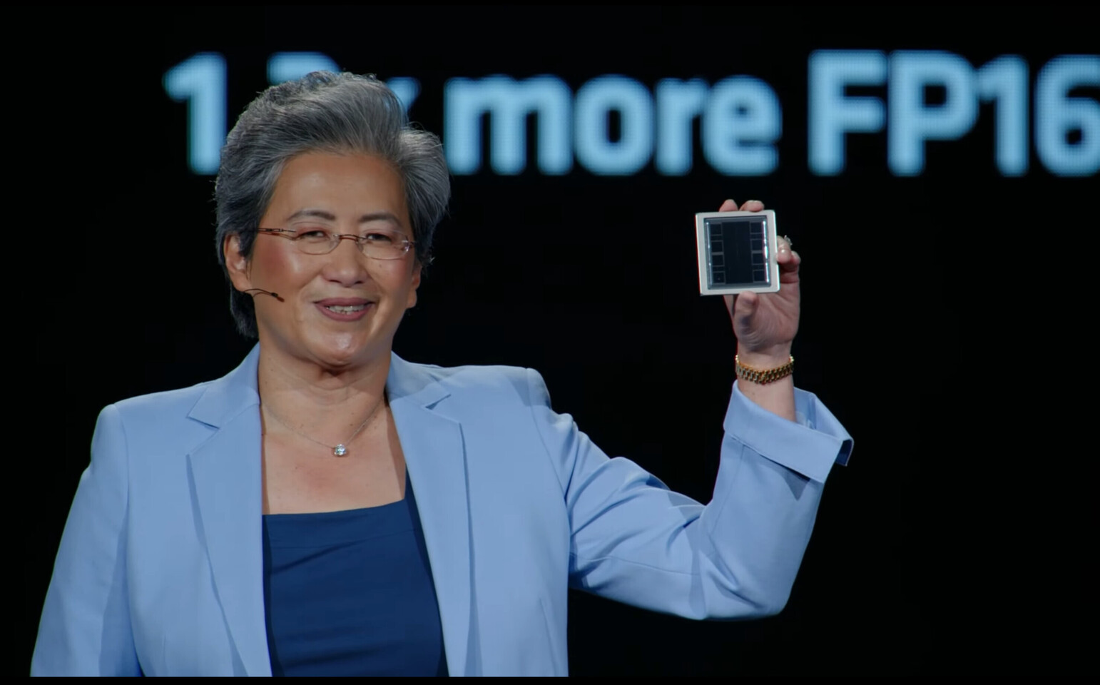
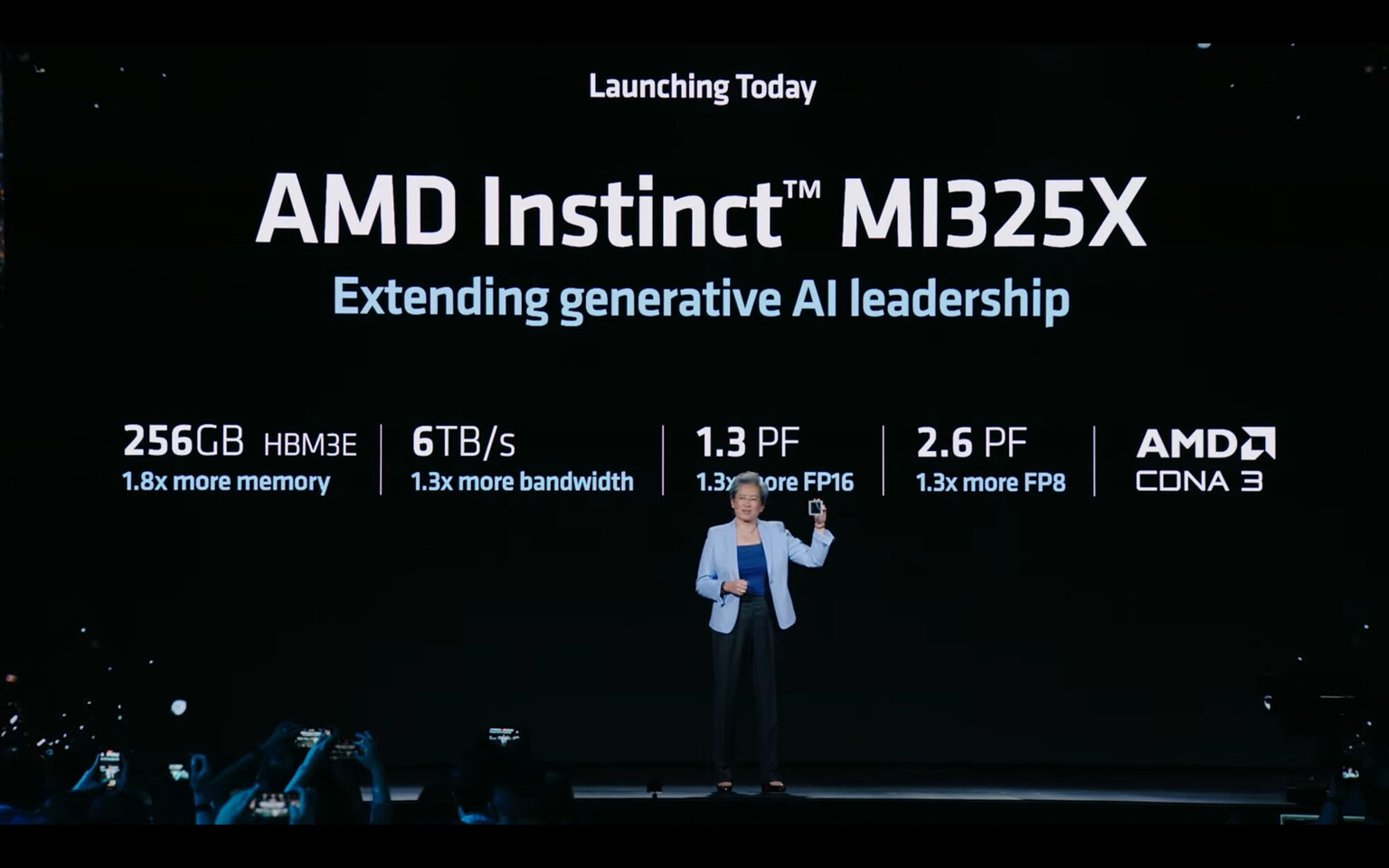
ASRock Rack Inc., a leading innovative server company, announced upgrades to its extensive lineup to support AMD EPYC 9005 Series processors. Among these updates is the introduction of the new 6U8M-TURIN2 GPU server. This advanced platform features AMD Instinct MI325X accelerators, specifically optimized for intensive enterprise AI applications, and will be showcased at AMD Advancing AI 2024.
ASRock Rack Introduce GPU Servers Powered by AMD EPYC 9005 series processors
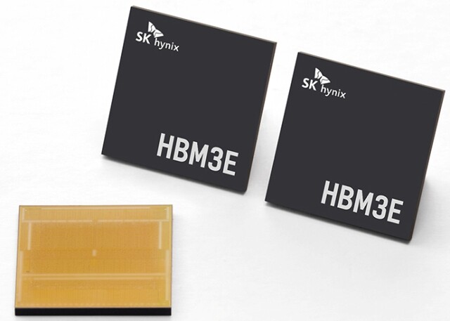
AMD today revealed the 5th Generation AMD EPYC processors, offering a wide range of core counts (up to 192 cores), frequencies (up to 5 GHz), and expansive cache capacities. Select high-frequency processors, such as the AMD EPYC 9575F, are optimized for use as host CPUs in GPU-enabled systems. Additionally, the just launched AMD Instinct MI325X accelerators feature substantial HBM3E memory and 6 TB/s of memory bandwidth, enabling quick access and efficient handling of large datasets and complex computations.
ASRock Rack Introduce GPU Servers Powered by AMD EPYC 9005 series processors
AMD today revealed the 5th Generation AMD EPYC processors, offering a wide range of core counts (up to 192 cores), frequencies (up to 5 GHz), and expansive cache capacities. Select high-frequency processors, such as the AMD EPYC 9575F, are optimized for use as host CPUs in GPU-enabled systems. Additionally, the just launched AMD Instinct MI325X accelerators feature substantial HBM3E memory and 6 TB/s of memory bandwidth, enabling quick access and efficient handling of large datasets and complex computations.