While memory prices continue to fall, allowing gamers and hardware enthusiasts everywhere to splurge on memory, it would seem as though this "golden age" of cheap memory is coming to an end. Hynix, mainly thanks to ridiculously low DRAM prices, reported a net loss of a half billion dollars last year. Hynix is also none too happy to announce that they do not expect things to get much better. DRAM prices are low/falling, and are expected to stay that way for quite some time. There are currently rumors that Hynix may consider exiting the memory business, despite strong sales in NAND flash technology.
Hynix Semiconductor (Hynix) announced it has received the validation from Intel Corporation on its 1Gb DDR2 DRAM with company's leading edge 50nm-class process technology. The production efficiency of Hynix's 50nm-class 1Gb DDR2 DRAM products is increased by 50% over its 60nm-class process technology and the lower costs of production are expected accordingly. Hynix adopts new technologies of "three-dimensional transistor" architecture and "W-DPG (Dual Poly Gate)" technology. These technologies significantly minimize leakage to further reduce overall power consumption and increase performance by optimizing its speed. The adoption of technologies will be extended to DDR3 DRAM and the mass production of validated 1Gb DDR2 DRAM as well as DDR3 products will begin in the second half of next year. As the demand for higher capacity memory is expected to grow, Hynix plans to enhance capacity on the 50nm-class products in order to suit needs from the market. Hynix's 50nm-class DDR2 DRAM processing technology will be also used in producing various applications not only mass storage PC DRAM but also Graphic DRAM, Mobile DRAM.
Hynix Semiconductor today introduced the industry's first 1 Gigabit GDDR5 Graphics DRAM. The industry's first 1Gb GDDR5 from Hynix is also the fastest and highest density graphics memory available. It operates at 5Gbps bandwidth and processes up to 20 Gigabytes of data per second with a 32-bit I/O, ideal in applications with high definition video and cinematic and photo-realistic graphics content. A bandwidth of 20 Gigabytes per second offered by the Hynix 1Gb GDDR5 can process more than 20 hours of DVD quality video.
Ovonyx and Hynix Semiconductor today announced that they have entered into a long-term license agreement for memory products under Ovonyx' patents and intellectual property relating to Phase Change Memory (PCM) technology. The agreement also provides that Ovonyx will actively support Hynix' program to develop phase change memory products.
South Korea's Hynix Semiconductor, the world's second-biggest maker of memory chips, said it stopped supplying computer memory chips through the spot market to defend against plummeting prices. Hynix will stop supplying memory chips effective September, without providing exact date. According to research firm Dramexchange, spot prices of some key DRAM chips have declined more than 10 percent over the last 10 days alone.
Hynix Semiconductor today announced it has received validation on its DDR3 memory components and modules from Intel. The newly-validated DDR3 products are 1GB DDR3 SDRAM Unbuffered-DIMMs manufactured on 80nm process technology. These devices have operating speeds from 800MHz to 1066MHz with reduced voltage to 1.5V. These speeds are offered in latency combinations of 5-5-5 and 6-6-6 for the 800MHz, and 7-7-7 for the 1066MHz memory modules. Mass production of the 1GB DDR3 on the 80nm line will begin in the third quarter of this year. Hynix plans to manufacture the product on a 66nm process beginning in late 2007.
Hynix Semiconductor Inc. and Toshiba Corporation announced today that they have signed patent cross licensing and product supply agreements covering semiconductor technology. Under the agreements, Hynix and Toshiba will be cross licensed to use one another's semiconductor patents. The agreements settle all pending patent-related litigation between the companies in the U.S. and Japan, including that before the U.S. International Trade Commission. Mr. OC Kwon, Senior Vice President, Hynix Semiconductor Inc. said, "We believe the agreements will become a good foundation for our two companies to build a mutually beneficial business relationship in the future." Mr. Shozo Saito, Corporate Vice President and Executive Vice President of Semiconductor Company, Toshiba Corporation, said, "The signing of the agreements is a positive step for both companies. With litigation behind us, and through these agreements, we can now strengthen our respective businesses."
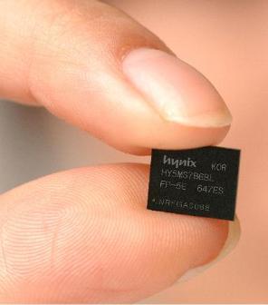
Hynix Semiconductor, Inc., today announced it has developed the industry's fastest 185MHz 512Megabit mobile DDR SDRAM with ECC (Error Correction Code). The built in ECC, similar to that used in NAND Flash, ensures data integrity while reducing current consumption by almost 50%. At 185MHz clock speed, the fastest in the industry, a throughput of up to 1.5Gbytes of data per second can be attained with a 32-bit I/O. The ECC feature in this product allows for the extension of the refresh interval which in turn significantly reduces power consumption. Additionally, the 512Mb ECC Mobile DDR offers the traditional low power features necessary for a wide range of mobile applications.
Hynix Develops 2GB DDR2-800 Memory Modules
Hynix has developed a 2GB DDR2 memory module with operating speeds of 800 MHz, which makes it the world's first in memory industry. The 2-Gbyte DDR2 module is based on 90-nanometer process technology using advanced wafer-level packaging technology (WLP). Hynix did not say precisely when the new memory modules will start mass production.
A batch of about NT$20 million (US$306,000) worth of DDR chips (from Hynix Semiconductor) was stolen yesterday in Taoyuan, Taiwan. The 20 boxes filled with DDR chips were robbed while in transit, with most of the chips being 400MHz frequency parts. This DDR chips were being delivered to distributors, though ownership of the chips is still unknown. A Chinese-language Economic Daily News (EDN) report cited sources as saying that three robbers staged an accident with the truck transporting the chips, and then subdued the driver using a machete and taser gun. The thieves were seen headed to the airport and the batch of chips are likely headed to China, the report said.
Hynix Semiconductor has developed the world's first 800 MHz memory module using 60nm 1GB DDR2 DRAM. The chipmaker received approval for its 60nm DRAM chip from Intel in October and has now developed the 60nm DDR2 memory module this time, passing Intel's Advanced Validation Lab (AVL) test. The new memory chip comes in two types: one with a speed of 800 MHz and the other with a speed of 667 MHz. It also helps hike productivity by a whopping 50 percent, the chipmaker says. In addition, such cutting edge technologies as a "three-dimensional" transistor and three-layered metal allocation boost storage capacity and processing speeds. Hynix is expected to start mass production in the first half of 2007 and use the new memory chip in making high density DRAM components and high performance products such as graphic and mobile DRAMs.
Hynix today announced it has developed the world's fastest and smallest 512Megabit mobile DRAM. This product meets JEDEC standards and operates at 200MHz - the fastest in the industry. By using 32-bit wide I/Os, Hynix's 512Mb mobile DDR SDRAM processes 1.6Gbytes (400 bps x32) of data per second, which is approximately 1.5 times faster than speed of the company's existing mobile DRAM products. The new product is expected to enhance the company's competitiveness in mobile applications, which is driving the trend towards miniaturization(8mm x 10mm). Moreover, Hynix is expected to combine 512Mb mobile DRAM and NAND Flash in a multi-chip package (MCP), which will enable the design of slimmer mobile phones.