News Posts matching #Hynix

Return to Keyword Browsing

SK Hynix Announces the Gold S31 Consumer SATA SSD

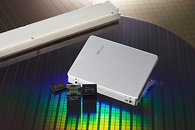
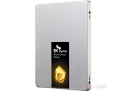
SK hynix Inc. announced today the launch of its "Gold S31" solid-state drive (SSD). Gold S31 (SATA III - first generation) is the first of the Company's new SuperCore series of consumer SSDs, an internal drive lineup based on SK hynix's core technology. With its speed and reliability, SK hynix's Gold S31 will be a perfect choice for all PC users, particularly for gamers, designers, and content creators. Gold S31 pushes the limits on high-performance SSDs, providing users the next level of speed with sequential read speeds up to 560 MB/s, as well as superior quality, reliability, and five-year warranty.

The 2.5-inch drive supports the SATA III interface based on 3D NAND Flash technology, and is now available in 1 TB, 500 GB and 250 GB capacities on Amazon US. All key components in Gold S31, from NAND Flash and built-in controller to DRAM and firmware, were designed and produced by SK hynix. The in-house components are built for robust performance and reliability.
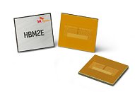
SK Hynix Announces its HBM2E Memory Products, 460 GB/s and 16GB per Stack

SK Hynix Inc. announced today that it has developed HBM2E DRAM product with the industry's highest bandwidth. The new HBM2E boasts approximately 50% higher bandwidth and 100% additional capacity compared to the previous HBM2. SK Hynix's HBM2E supports over 460 GB (Gigabyte) per second bandwidth based on the 3.6 Gbps (gigabits-per-second) speed performance per pin with 1,024 data I/Os (Inputs/Outputs). Through utilization of the TSV (Through Silicon Via) technology, a maximum of eight 16-gigabit chips are vertically stacked, forming a single, dense package of 16 GB data capacity.

SK Hynix's HBM2E is an optimal memory solution for the fourth Industrial Era, supporting high-end GPU, supercomputers, machine learning, and artificial intelligence systems that require the maximum level of memory performance. Unlike commodity DRAM products which take on module package forms and mounted on system boards, HBM chip is interconnected closely to processors such as GPUs and logic chips, distanced only a few µm units apart, which allows even faster data transfer.

SK Hynix Named as Memory & Storage Solutions Partner to Support Latest AMD EPYC 7002 Series

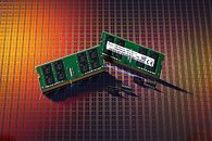
SK Hynix Inc. announced today that its DRAM and Enterprise SSD (eSSD) solutions, including the up-to-date 1Y nm 8 Gb DDR4 DRAM, have been fully tested and validated with the new AMD EPYC 7002 Generation Processors, which were unveiled during AMD's launch event on August 7. The Company has worked closely with AMD to provide memory solutions fully compatible with the 2nd Gen AMD EPYC Processors, targeting high performance data centers.

The SK Hynix DDR4 DRAM supports the maximum speed of 3200 Mbps of the 2nd Gen EPYC Processors, which will increase memory performance more than 20% compared to the 1st Gen AMD EPYC Processors. The Company's various DDR4 DRAM solutions, based on the 1Xnm and 1Y nm technology with density of 8 Gb and 16 Gb, have been fully tested and validated with the 2nd Gen EPYC Processors. SK Hynix provides high-density DIMMs with density over 64 GB to support up to 64 cores per socket in the 2nd Gen EPYC.

SK Hynix also provides a full line-up of SATA and PCIe from 480 GB to 8 TB, which have also been validated and tested with the 2nd Gen EPYC. SK Hynix's eSSD solutions are optimized for the latest data center's read-intensive and mixed workload environment.

SK Hynix Starts Mass-Producing World's First 128-Layer 4D NAND

SK Hynix Inc. announced today that it has developed and starts mass-producing the world's first 128-Layer 1 Tb (Terabit) TLC (Triple-Level Cell) 4D NAND Flash, only eight months after the Company announced the 96-Layer 4D NAND Flash last year.

The 128-Layer 1 Tb NAND chip offers the industry's highest vertical stacking with more than 360 billion NAND cells, each of which stores 3 bits, per one chip. To achieve this, SK Hynix applied innovative technologies, such as "ultra-homogeneous vertical etching technology," "high-reliability multi-layer thin-film cell formation technology," and ultra-fast low-power circuit design, to its own 4D NAND technology.

SK Hynix Reports Second Quarter 2019 Results

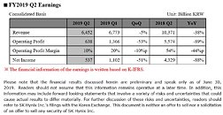
SK hynix Inc. today announced financial results for its second quarter 2019 ended on June 30, 2019. The consolidated second quarter revenue was 6.45 trillion won while the operating profit amounted to 638 billion won and the net income 537 billion won. Operating margin for the quarter was 10% and net margin was 8%.

As demand recovery did not meet expectations and price declines were steeper than expected, the revenue and the operating profit in the second quarter fell by 5% and 53%, respectively, quarter-over-quarter (QoQ). DRAM bit shipments increased by 13% QoQ as the Company actively responded to the mobile and PC DRAM markets, where demand growth was relatively high. However, DRAM prices remained weak and the average selling price dropped by 24%. For NAND Flash, the bit shipments increased by 40% QoQ because of demand recovery due to price declines, while the average selling price decreased by 25%.

SK Hynix Starts Mass-Producing World's First 128-Layer 4D NAND, Working on 176-Layer NAND

SK hynix Inc. announced today that it has developed and started mass-producing the world's first 128-Layer 1 Tb (Terabit) TLC (Triple-Level Cell) 4D NAND Flash, only eight months after the Company announced the 96-Layer 4D NAND Flash last year.

The 128-Layer 1 Tb NAND chip offers the industry's highest vertical stacking with more than 360 billion NAND cells, each of which stores 3 bits, per one chip. To achieve this, SK hynix applied innovative technologies, such as "ultra-homogeneous vertical etching technology," "high-reliability multi-layer thin-film cell formation technology," and ultra-fast low-power circuit design, to its own 4D NAND technology.

The new product provides the industry's highest density of 1 Tb for TLC NAND Flash. A number of companies including SK hynix have developed 1 Tb QLC (Quad-Level Cell) NAND products, but SK hynix is the first to commercialize the 1 Tb TLC NAND Flash. TLC accounts for more than 85% of the NAND Flash market with excellent performance and reliability.
SK Hynix Begins Sampling 96-layer 4D QLC NAND Flash Memory

SK Hynix Inc., announced today that it has delivered samples of new 1Tb (Terabit) QLC (Quadruple Level Cell) product to major SSD (Solid State Drive) Controller companies. The Company applied its own QLC technology to its world's first 96-Layer "CTF (Charge Trap Flash) based 4D (Four-Dimensional) NAND Flash (or 4D NAND)." SK Hynix intends to expand its NAND portfolio to 96-layer-based 1Tb QLC products in time for the QLC market opening and strengthen its responsiveness to the next-generation high-density memory market.

QLC stores four bits of data in one NAND cell, allowing higher density compared to TLC (Triple Level Cell) that stores three bits per cell. Using QLC, it is possible to develop high-density products with cost competitiveness. SK Hynix is able to secure the industry's top-level cost competitiveness through this product, which has reduced the area to less than 90% of the existing 3D-based QLC products.

SK Hynix Completes Expanded Fab (C2F) in Wuxi, China

SK Hynix Inc. today announced that it held a ceremony celebrating the completion of an expanded fabrication plant (or 'C2F') in Wuxi, China, on April 18th. C2F is an expansion of the existing DRAM production line, C2, in Wuxi. The Company decided to expand its production line in 2016 in order to solve the shortage of production space due to technology migration. About 500 people attended the ceremony, including Li Xiaomin, Party Secretary of Wuxi, Guo Yuanqiang, Vice Governor of Jiangsu, Choi Youngsam, Consul-General in Shanghai, Lee Seok-hee, Chief Executive Officer of SK Hynix, and representatives of clients and business partners.

SK Hynix signed a contract with Wuxi City, Jiangsu Province, China, in 2004 to establish a local factory and completed the production line (C2) in 2006 to start producing DRAM. C2 is the Company's first 300mm FAB and has played a major role in SK Hynix's growth to date. However, with technology scaling, the number of processes has increased and the equipment has become larger, which led to the shortage of the cleanroom space. SK Hynix, therefore, has invested a total of 950 billion KRW from June 2017 to April 2019 to secure additional production space.

SK Hynix Inc. Reports First Quarter 2019 Results

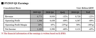
SK Hynix Inc. today announced financial results for its first quarter 2019 ended on March 31, 2019. The consolidated first quarter revenue was 6.77 trillion won while the operating profit amounted to 1.37 trillion won and the net income 1.1 trillion won. Operating margin for the quarter was 20% and net margin was 16%.

Because of a faster-than-expected price decline and lower shipments due to slowing memory demand, the revenue and the operating profit in the first quarter fell by 32% and 69%, respectively, quarter-over-quarter (QoQ). Due to seasonal slowdown and conservative server purchases, DRAM bit shipments decreased by 8% QoQ. The average selling price dropped by 27%. For NAND Flash, the average selling price decreased by 32% due to high inventory levels and intensifying competition among suppliers. The bit shipments declined by 6% QoQ.

SK Hynix Fellow Says PC5 DDR5 by 2020, DDR6 Development Underway

The PC5 DDR5 main memory standard could enter the market by 2020, according to SK Hynix research fellow Kim Dong-Kyun. The first such memory standard will be DDR5-5200, which offers nearly double the bandwidth of DDR4-2666. "We are discussing several concepts of the post DDR5," he said. "One concept is to maintain the current trend of speeding up the data transmission, and another is to combine the DRAM technology with system-on-chip process technologies, such as CPU," he added, without offering any additional information. SK Hynix had in 2018 developed a working prototype of a 16-gigabit (2 GB) DDR5 DRAM chip ticking at 5200 MT/s, at 1.1 Volts. A 64-bit wide memory module made with these chips could offer bandwidth of 41.6 GB/s.

SK Hynix is developing its own innovations that could make its DDR5 chips more advanced than the competition without going off-standard. "We have developed a multi-phase synchronization technology that enables keeping the voltage during a high-speed operation in a chip at a low level by placing multiple phases within the IP circuit, so the power used on each phase is low but the speed is high when combined," Kim said. He also mentioned that development of the DDR6 PC memory standard is already underway, with the design goals of doubling bandwidth and densities over DDR5. Advancements in DRAM are propelled not just by the PC ecosystem, but also handhelds and self-driving car electronics.

SK Hynix Develops 10 nm-class 8 Gb DDR4 DRAM

SK Hynix Inc. announced that it has developed 1Ynm 8Gb (Gigabits) DDR4 (Double Data Rate 4) DRAM. The productivity of this product is increased by 20% and the power consumption reduced by more than 15%, compared to the previous generation, 1Xnm DRAM. It also supports a data transfer rate of up to 3,200Mbps, which is the fastest data processing speed in DDR4 interface. The Company adopted a '4-Phase Clocking' scheme, which doubles the clock signal to boost data transfer speed and stability.
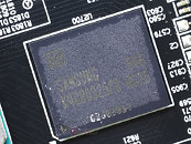
SK Hynix also introduced its own 'Sense Amp. Control' technology to reduce power consumption and data errors. With this technology, the Company successfully enhanced the performance of the sense amplifier. SK Hynix improved the transistor structure to lower the possibility of data errors, a challenge that accompanies technology shrink. The Company also added a low-power power supply to the circuit to prevent unnecessary power consumption.

NAND Flash Prices May See Further Drops in 2019, DRAM to Remain Flat

Solid-state drives are cheaper than ever, thanks to systematic decline in NAND flash prices owing both to oversupply and increases in densities. NAND flash prices have already declined by 50 percent over 2018, according to a DigiTimes report, and will continue to slide through 2019. ADATA chairman Simon Chen commented that NAND flash makers haven't slowed down capacity expansions, and 2019 could witness an even bigger drop in prices than 2018.

Major NAND flash makers such as IMFlash Technology, SK Hynix, Samsung, Western Digital, Toshiba, have already taped out their 96-layer 3D NAND flash products, which could enter volume production in the first half of 2019. This could impact prices of existing swelling inventories of products based on 64-layer NAND flash. In theory, the 96-layer chips introduce 50 percent increases in densities. Adoption of newer technologies such as QLC (4 bits per cell) will expand densities even further. The same report also projects that DRAM prices could largely remain flat throughout 2019. Most NAND flash makers also happen to make DRAM, and could balance their NAND flash losses with DRAM profits.

SK Hynix Unveils 4D NAND Flash Memory Concept

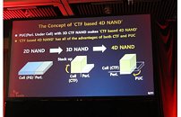
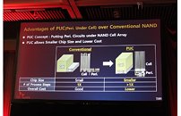
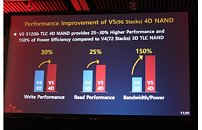
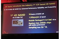
3D NAND flash revolutionized flash storage as it used the third dimension (height) to stack multiple NAND flash layers, resulting in infinitesimally smaller footprint and reduced costs. SK Hynix believes that a "4-dimensional" NAND flash package is possible. Don't worry, such a stack doesn't look like a tesseract. Conventional 3D NAND flash relies on stacks of charge-trap flash (CTF) cells spatially located alongside its periphery block (which is responsible for wiring out each of the layers of the CTF stack). On a 2-D plane you'd be spending substrate real-estate on both the CTF and periphery block.

SK Hynix believes that the periphery block can be stacked along with the CTF stack, with microscopic vias wiring up the stack along the periphery, reducing the footprint of each cell stack. 4D stacking will also allow for greater number of CTF stacks per cell. Just to be clear, we're talking about stacks of cell and not stacks of NAND flash dies. The V5 cell-stack in SK Hynix's design entails 4 cells and periphery blocks sandwiched. The first implementation of this technology is a 96-layer 4D NAND flash chip with 512 Gb of capacity and TLC (3 bits per cell) density, although the technology is ready for QLC cells. This 512 Gb chip will begin sampling by the end of 2018, and the company is already working on a 1 Tb chip for 2019.

SK Hynix to Build New $3.5B Plant for Future Memory Technologies

SK Hynix Inc. today announced that the Company will construct a new semiconductor fabrication plant (or 'the FAB') at its headquarters in Icheon, Gyeonggi-do, to respond to growing demand for memory chips and to secure a future growth engine.

Construction on the 53,000 m² site in Icheon will begin late 2018 and is slated to be completed in October 2020. SK Hynix will invest 3.5 trillion won in the FAB. The production portfolio of the FAB shall be decided considering future market conditions as well as the Company's technology capability.

Chinese DRAM Companies Stealing DRAM IP From Samsung and SK Hynix

It's not just Micron, but also Korean DRAM giants Samsung and SK Hynix, that are the latest victims of large-scale industrial espionage by Chinese DRAM makers to steal vital DRAM intellectual property (IP), according to Korea Times. Today's DRAM makers build their products on IP acquired over decades, and that is time Chinese companies do not have, and aren't willing to license from established DRAM makers, either.

"Samsung Electronics and SK Hynix have become the target of industrial espionage by Chinese memory chip manufacturers. In semiconductors, patents are critical to the cost structure. The companies have to protect what they have spent decades building. The result is Chinese companies are attempting to infringe on Samsung and SK patents," said a Korean official involved in the investigation of IP theft.

Samsung, Micron, and Hynix Reportedly Slapped with Colossal Antitrust Fines

China's Anti-Monopoly Bureau of Ministry of Commerce visited Samsung Electronics, SK Hynix, and Micron Technology last year to express its concerns over the high prices of DRAM. Unfortunately, these meetings yielded no results as DRAM prices continued to skyrocket in the first quarter of this year. With their patience exhausted, Chinese antitrust regulators finally launched an investigation into Samsung, Micron, and Hynix, which collectively owns 90% of the global DRAM pie. The three DRAM vendors are allegedly cooperating with the Chinese authorities to shed some light into the whole DRAM price fixing matter. If found guilty, they could face fines between $800 million to $8 billion. The estimated fines were calculated based on the companies' DRAM sales in China between 2016 and 2017.

Whether you believe in coincidence or not, Samsung, Micron, and Hynix have a long history of being partners in crime. The trio, along with Infineon and Elpida Memory, conspired to fix prices on DRAM in the United States from April 1999 and June 2002. Infineon pleaded guilty in 2004 and was fined $160 million. Hynix cracked shortly afterwards and paid $185 million in fines. Elpida got off the hook easy with a $84 million fine, while Samsung took the biggest hit paying up to $300 million. Curiously, Infineon called it quits shortly after the incident, and Micron later acquired Elpida. In other news, China aims to become self-sufficient in the IC department by supporting local manufacturers like Yangtze Memory Technologies (YMTC).

Samsung, Micron, and Hynix Accused of DRAM Price Fixing

Law firm Hagens Berman has filed a class action lawsuit against Samsung, Micron, and Hynix in the US District Court for the Northern District of California. According to the firm's investigation, the three DRAM manufacturers conspired to limit the supply of DRAM chips between 2016 and 2017 with the purpose of inflating their prices. The firm affirmed that DRAM saw a 47 percent increase in price during 2017, which made it the largest jump ever in the last 30 years. As noted by the filing, Samsung, Micron and Hynix collectively own 96 percent of the worldwide DRAM market as of 2017. The "conduct changed abruptly" when the Chinese government launched an investigation to look into the matter. This class action is opened to consumers in the U.S. who've purchased a device that uses DRAM between July 1, 2016 and February 1, 2018.

"What we've uncovered in the DRAM market is a classic antitrust, price-fixing scheme in which a small number of kingpin corporations hold the lion's share of the market," stated Hagens Berman managing partner Steve Berman. "Instead of playing by the rules, Samsung, Micron and Hynix chose to put consumers in a chokehold, wringing the market for more profit."

SK Hynix Announces Availability of 16 Gb DDR4 Chips, up to 256 GB DIMMs

Sk Hynix has added to its product catalog single-die 16 Gb DDR4 memory chips, which should enable a two-fold increase in maximum memory capacity per single DIMM. This allows SK Hynix to sell same-capacity chips with fewer memory semiconductor dies, due to the increase in storage density, and to increase maximum memory capacity at the same memory die populations as before. The benefits are lower power consumption (due to the reduced number of memory dies to power), and the possibility of putting together either dual-ranked 64 GB modules, quad-ranked 128 GB LRDIMMs and octal-ranked 256 GB LRDIMMs. That last part is the most important: theoretically, the maximum amount of memory on top Intel or AMD server platforms could double, which could enable up to 4 TB RAM in EPYC systems, for example. And as memory-hungry as big data applications have become, there's ever need for higher memory capacity.
SK Hynix's 16 Gb DDR4 chips are organized as 1Gx16 and 2Gx8 and supplied in FBGA96 and FBGA78 packages, respectively. Current 16 Gb density speeds stand at DDR4-2133 CL15 or DDR4-2400 CL17 modes at 1.2 V. SK Hynix plans increase the available frequencies in the third quarter of this year, adding DDR4-2666 CL19 to the lineup.

SK Hynix Marks its 8Gb GDDR6 Memory Chips "Available" in Latest Catalog Update

SK Hynix, the other Korean DRAM and NAND flash giant than Samsung, updated its DRAM product catalog to reflect immediate availability of its 8-gigabit (1 GB) GDDR6 memory chips. The company is selling four SKUs, part "H56C8H24MJR-S2C" in 14 Gbps and 12 Gbps variants; and part "H56C8H24MJR-S0C" in 12 Gbps and 10 Gbps variants. The -S2C chips are more energy efficient, in achieving 14 Gbps at 1.35V and 12 Gbps at 1.25V; while the -S0C achieves 12 Gbps at 1.35V, and 10 Gbps at 1.25V. Unless NVIDIA decides that the GTX 1080-successor should feature 16 GB of memory, the company could be in the market for 8 Gb GDDR6 chips.

Meanwhile, rival Samsung announced that it began mass-production of 16 Gb (2 GB) GDDR6 memory chips, which should enable 16 GB of memory across a 256-bit memory interface, or 8 GB over a 128-bit interface. Samsung's latest chips not only have double the density as SK Hynix's, but also tick faster, at 18 Gbps, with a voltage of 1.35V. It is widely expected that GDDR6 will be the dominant memory standard for entry, mainstream, and even high-end graphics cards, which launch through 2018-19. NVIDIA is expected this year to launch its new "Volta" graphics architecture across various consumer-graphics market-segments.

4Q DRAM Sales Put Exclamation Point On An Amazing Year of Growth

Throughout 2017, DRAM manufacturers faced pressure to boost output of their devices-particularly high-performance DRAM used in data center servers, and low-power high-density DRAM used in smartphones and other mobile products. Strong, ongoing demand put significant upward pressure on DRAM average selling prices. This trend continued into 4Q17 and is expected to drive quarterly DRAM sales to an all time high mark of $21.1 billion (Figure 1), capping an incredible year of growth in which DRAM sales set a new all time high sales mark each quarter. The forecast $21.1 billion sales level in 4Q17 would be an increase of 65% compared to the $12.8 billion DRAM market of 4Q16.

Toshiba Sells its Memory Business to Bain Capital for $18 Billion

Toshiba today announced that it has signed an agreement with a consortium led by Bain Capital to sell its memory business for JPY 2 trillion (approximately USD $18 billion). The consortium includes Korean memory giant SK Hynix, which contributed JPY 395 billion (nearly 20 percent) of the consortium's investment toward acquisition of Toshiba Memory Corp. Apple and Dell are the other members of the consortium.

Toshiba Corporation (erstwhile parent of Toshiba Memory Corp.) continues to hold a 40.2 percent stake, which along with another Japanese company, Hoya Corporation, holding a 9.9 percent stake, ensure that Japanese firms hold 50.1 percent of the business, keeping Japanese regulators happy. The Bain Capital-led consortium will hold a 49.9 percent stake, ensuring that Toshiba Memory Corp. stays afloat, and away from rival Western Digital, which has dragged Toshiba to a multitude of international courts and arbitrators. Apart from SK Hynix, the Bain Capital-led consortium includes Apple and Dell, who feared they would lose DRAM and NAND flash price bargaining power if Toshiba Memory fell in the hands of Western Digital, which owns SanDisk.

WD Comments on Toshiba's Statement Regarding NAND Flash-Memory JV

Western Digital Corp. (NASDAQ: WDC) today commented on Toshiba Corporation's ("Toshiba") statement regarding the transfer of its interests in its NAND flash-memory joint ventures operated with Western Digital's SanDisk subsidiaries ("JVs"):

"We are disappointed that Toshiba would take this action despite Western Digital's tireless efforts to reach a resolution that is in the best interests of all stakeholders. Throughout our ongoing dialogue with Toshiba, we have been flexible, constructive and have submitted numerous proposals to specifically address Toshiba's stated concerns. Our goal has been - and remains - to reach a mutually beneficial outcome that satisfies the needs of Toshiba and its stakeholders, and most importantly, ensures the longevity and continued success of the JVs.

Furthermore, it is surprising that Toshiba would continue to pursue a transaction with a consortium led by Korea-based SK Hynix Inc. and Bain Capital Japan without SanDisk's consent, as the language in the relevant JV agreements is unambiguous, and multiple courts have ruled in favor of protecting SanDisk's contractual rights. We remain confident in our ability to protect our JV interests and consent rights."

Graphics Memory Prices Surge 30% in August, Could Affect Graphics Card Prices

The DRAM industry is experiencing an acute shortage of various classes of GDDR memory (graphics DDR), which could affect graphics card prices come Holiday. Supplier quotes for various graphics memory components have risen by as much as 30.8% in August, from an average of USD $6.50 in July, to $8.50. Top graphics memory suppliers Samsung and SK Hynix have committed a bulk of their inventories to manufacturers of servers and mobile handsets, which triggered the price rally. Samsung is the largest supplier of graphics memory, with a 55 percent market-share, followed by SK Hynix at 35 percent, and Micron Technology at 10 percent.

Sk Hynix Begins Mass Production of 72-Layer 3D NAND

After announcing their intention to begin mass production of their latest 72-Layer 3D NAND Flash back in April, SK Hynix has now confirmed that it has entered mass production of the high density NAND modules. Apparently, SK Hynix has already achieved the much sought-after "golden yield" ratios, where the semiconductor yield is now at such a level that it is advantageous to finally enter mass production. Apparently, SK Hynix's leadership was fearful of not being able to achieve the golden yield in a timely manner after their announcement of the technology only three months ago; however, after its "management team and engineers repeatedly spent nights doing research, yield went up vertically and has become comparable to Samsung Electronics'" own yield - and as you know, Samsung is kind of the golden standard when it comes to NAND technology.

According to industry sources, SK Hynix is already mass-producing SSDs (Solid State Drives) with the company's own controllers and firmware which leverage this new 72-layer 256Gb NAND flash memory. This is a welcome change for the company which should allow it to increase revenue, since this is the first time controllers are developed in-house. The company is also said to be already producing eMMC (embedded Multimedia Card) for mobile devices based on this technology, with supply already arriving to its customers.

Sapphire Makes Mining-Oriented Graphics Cards Available for Pre-Order

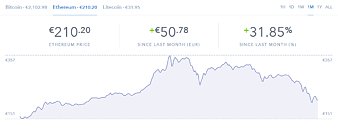
Ah mining. The revival of an old craze. Who doesn't want to make their room's temperature increase to insane levels over the summer in order to cash in on the mining wagon? Who doesn't want to pull their hardware by the ankles and wrists, stretching it in utilization so as to maintain the PoW (proof of Work) cryptographic security in cryptocurrencies? Apparently, a not insignificant number of users and would-be miners does want that. That has, in turn, placed a whole lot of pressure on the graphics card market from both AMD and NVIDIA, with prices climbing and skyrocketing for graphics cards in the $200-$400 price ranges, as you know. It remains to be seen whether the flow of new miners decreases somewhat now, considering the recent market correction (read: dip) in the cryptocurrency market value (down around 42% from the all-time high of 357€ [~$400] of June 12th.)

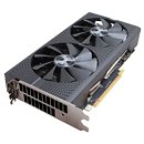
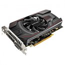
After ASUS, it would seem like it's Sapphire's time to try and sway miners from their consumer-oriented, gaming graphics cards, through the launch of five different graphics cards models especially geared for mining. These are currently available for pre-order on Overclockers UK, and there are five different products in total, one based of RX 560 silicon, and four different takes on the RX 470 silicon (no, that's not a typo; it really is the 400 series.)
Return to Keyword Browsing
Dec 18th, 2024 04:30 EST change timezone

New Forum Posts

Popular Reviews

Controversial News Posts