Thursday, August 9th 2018

SK Hynix Unveils 4D NAND Flash Memory Concept
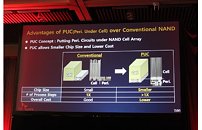
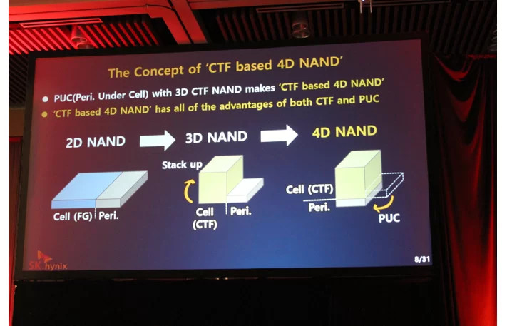
3D NAND flash revolutionized flash storage as it used the third dimension (height) to stack multiple NAND flash layers, resulting in infinitesimally smaller footprint and reduced costs. SK Hynix believes that a "4-dimensional" NAND flash package is possible. Don't worry, such a stack doesn't look like a tesseract. Conventional 3D NAND flash relies on stacks of charge-trap flash (CTF) cells spatially located alongside its periphery block (which is responsible for wiring out each of the layers of the CTF stack). On a 2-D plane you'd be spending substrate real-estate on both the CTF and periphery block.
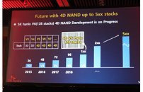
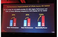
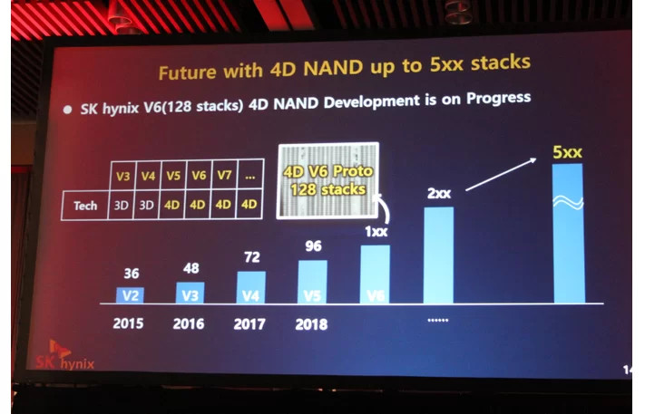
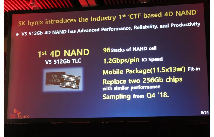
SK Hynix believes that the periphery block can be stacked along with the CTF stack, with microscopic vias wiring up the stack along the periphery, reducing the footprint of each cell stack. 4D stacking will also allow for greater number of CTF stacks per cell. Just to be clear, we're talking about stacks of cell and not stacks of NAND flash dies. The V5 cell-stack in SK Hynix's design entails 4 cells and periphery blocks sandwiched. The first implementation of this technology is a 96-layer 4D NAND flash chip with 512 Gb of capacity and TLC (3 bits per cell) density, although the technology is ready for QLC cells. This 512 Gb chip will begin sampling by the end of 2018, and the company is already working on a 1 Tb chip for 2019.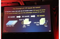

Source:
Tom's Hardware
SK Hynix believes that the periphery block can be stacked along with the CTF stack, with microscopic vias wiring up the stack along the periphery, reducing the footprint of each cell stack. 4D stacking will also allow for greater number of CTF stacks per cell. Just to be clear, we're talking about stacks of cell and not stacks of NAND flash dies. The V5 cell-stack in SK Hynix's design entails 4 cells and periphery blocks sandwiched. The first implementation of this technology is a 96-layer 4D NAND flash chip with 512 Gb of capacity and TLC (3 bits per cell) density, although the technology is ready for QLC cells. This 512 Gb chip will begin sampling by the end of 2018, and the company is already working on a 1 Tb chip for 2019.


15 Comments on SK Hynix Unveils 4D NAND Flash Memory Concept
oh, and the model t was only about 500 bucks not 50+ thousand$
thing is they promote this stuff as a sales pitch [opinion] what it comes down to is it all that at your house in your computer ? cause funny how in the end at your house it don't quite do as claimed in the promotions and reviews .
But the engineer in me wants to know how moving the wiring from besides the cell, under the cell can improve the performance. Because, going by what was released here, that doesn't compute.
Back to the car analogy, I can move the wiring inside a car as much as I want. It won't make it go any faster.
It might be as simple that the data path is improved somehow by doing this.
I guess we'll have to wait for a proper explanation once these products are available, but it's not like a company of this size would go out with something like if they hadn't tested it and seen a performance improvement.