News Posts matching #Hynix

Return to Keyword Browsing

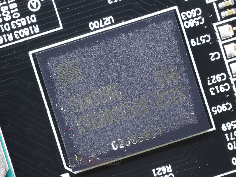
Toshiba Sells its Memory Business to Bain Capital for $18 Billion

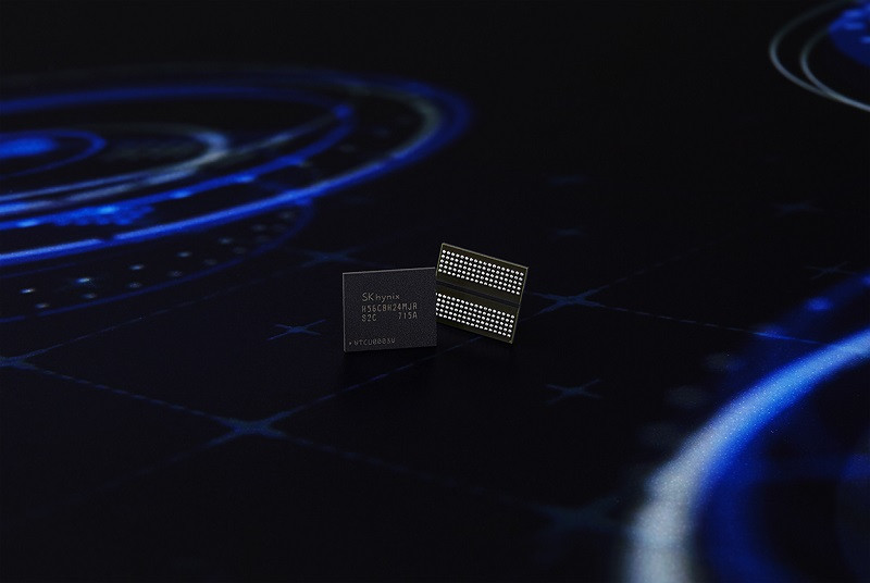
Toshiba today announced that it has signed an agreement with a consortium led by Bain Capital to sell its memory business for JPY 2 trillion (approximately USD $18 billion). The consortium includes Korean memory giant SK Hynix, which contributed JPY 395 billion (nearly 20 percent) of the consortium's investment toward acquisition of Toshiba Memory Corp. Apple and Dell are the other members of the consortium.

Toshiba Corporation (erstwhile parent of Toshiba Memory Corp.) continues to hold a 40.2 percent stake, which along with another Japanese company, Hoya Corporation, holding a 9.9 percent stake, ensure that Japanese firms hold 50.1 percent of the business, keeping Japanese regulators happy. The Bain Capital-led consortium will hold a 49.9 percent stake, ensuring that Toshiba Memory Corp. stays afloat, and away from rival Western Digital, which has dragged Toshiba to a multitude of international courts and arbitrators. Apart from SK Hynix, the Bain Capital-led consortium includes Apple and Dell, who feared they would lose DRAM and NAND flash price bargaining power if Toshiba Memory fell in the hands of Western Digital, which owns SanDisk.

WD Comments on Toshiba's Statement Regarding NAND Flash-Memory JV

Western Digital Corp. (NASDAQ: WDC) today commented on Toshiba Corporation's ("Toshiba") statement regarding the transfer of its interests in its NAND flash-memory joint ventures operated with Western Digital's SanDisk subsidiaries ("JVs"):

"We are disappointed that Toshiba would take this action despite Western Digital's tireless efforts to reach a resolution that is in the best interests of all stakeholders. Throughout our ongoing dialogue with Toshiba, we have been flexible, constructive and have submitted numerous proposals to specifically address Toshiba's stated concerns. Our goal has been - and remains - to reach a mutually beneficial outcome that satisfies the needs of Toshiba and its stakeholders, and most importantly, ensures the longevity and continued success of the JVs.

Furthermore, it is surprising that Toshiba would continue to pursue a transaction with a consortium led by Korea-based SK Hynix Inc. and Bain Capital Japan without SanDisk's consent, as the language in the relevant JV agreements is unambiguous, and multiple courts have ruled in favor of protecting SanDisk's contractual rights. We remain confident in our ability to protect our JV interests and consent rights."

Graphics Memory Prices Surge 30% in August, Could Affect Graphics Card Prices

The DRAM industry is experiencing an acute shortage of various classes of GDDR memory (graphics DDR), which could affect graphics card prices come Holiday. Supplier quotes for various graphics memory components have risen by as much as 30.8% in August, from an average of USD $6.50 in July, to $8.50. Top graphics memory suppliers Samsung and SK Hynix have committed a bulk of their inventories to manufacturers of servers and mobile handsets, which triggered the price rally. Samsung is the largest supplier of graphics memory, with a 55 percent market-share, followed by SK Hynix at 35 percent, and Micron Technology at 10 percent.

Sk Hynix Begins Mass Production of 72-Layer 3D NAND

After announcing their intention to begin mass production of their latest 72-Layer 3D NAND Flash back in April, SK Hynix has now confirmed that it has entered mass production of the high density NAND modules. Apparently, SK Hynix has already achieved the much sought-after "golden yield" ratios, where the semiconductor yield is now at such a level that it is advantageous to finally enter mass production. Apparently, SK Hynix's leadership was fearful of not being able to achieve the golden yield in a timely manner after their announcement of the technology only three months ago; however, after its "management team and engineers repeatedly spent nights doing research, yield went up vertically and has become comparable to Samsung Electronics'" own yield - and as you know, Samsung is kind of the golden standard when it comes to NAND technology.

According to industry sources, SK Hynix is already mass-producing SSDs (Solid State Drives) with the company's own controllers and firmware which leverage this new 72-layer 256Gb NAND flash memory. This is a welcome change for the company which should allow it to increase revenue, since this is the first time controllers are developed in-house. The company is also said to be already producing eMMC (embedded Multimedia Card) for mobile devices based on this technology, with supply already arriving to its customers.

Sapphire Makes Mining-Oriented Graphics Cards Available for Pre-Order

Ah mining. The revival of an old craze. Who doesn't want to make their room's temperature increase to insane levels over the summer in order to cash in on the mining wagon? Who doesn't want to pull their hardware by the ankles and wrists, stretching it in utilization so as to maintain the PoW (proof of Work) cryptographic security in cryptocurrencies? Apparently, a not insignificant number of users and would-be miners does want that. That has, in turn, placed a whole lot of pressure on the graphics card market from both AMD and NVIDIA, with prices climbing and skyrocketing for graphics cards in the $200-$400 price ranges, as you know. It remains to be seen whether the flow of new miners decreases somewhat now, considering the recent market correction (read: dip) in the cryptocurrency market value (down around 42% from the all-time high of 357€ [~$400] of June 12th.)

After ASUS, it would seem like it's Sapphire's time to try and sway miners from their consumer-oriented, gaming graphics cards, through the launch of five different graphics cards models especially geared for mining. These are currently available for pre-order on Overclockers UK, and there are five different products in total, one based of RX 560 silicon, and four different takes on the RX 470 silicon (no, that's not a typo; it really is the 400 series.)

No Relief for DRAM and NAND Shortages in Sight; Considerable Supply Only in 2018

DRAM prices have been high for quite some time now, due to a general increased demand over a slowly improving supply capability from manufacturers. Pricing of DRAM has been increasing (to the tune that if I wanted to double my memory capacity, I would have to pay double of what I paid a mere 11 months ago.) NAND pricing has been affected as well, with newer technologies such as 3D NAND not having a relevant impact on end user pricing as was expected, since tight supply and growing demand means process-level savings are dwarfed by the increasing prices on the balance of supply and demand.

Most of our woes can be traced back to high-end smartphones, which make use of up to 6 GB of RAM and have copious amounts of NAND memory. Now, reports are coming in that due to the iPhone 8's impending launch, supply is even tighter, with several firms being either unable to secure the amount of Ram they are looking for, or having to order in significant advance (futures speculation anyone?) Reuters is reporting that some clients have moved to 6-month supply agreements for their DRAM and NAND purchases, accepting higher prices than the customary quarterly or monthly deals, to make sure they get enough memory chips for their products.

GeIL Unveils AMD Edition Variants of its Entire DDR4 Memory Lineup

It turns out that the EVO X AMD Edition isn't GeIL's only AMD Ryzen-optimized DDR4 memory, with the company unveiling AMD Edition variants of pretty much all its DDR4 memory brands. This includes the EVO Potenza, EVO Spear, EVO Forza, Super Luce, Pristine, and DragonRAM series. Each of these "AMD Edition" branded memory kits has been stability-tested with AMD Ryzen processors, at their advertised clock speeds and timings. They come in a variety of speeds, including DDR4-2400, DDR4-2666, DDR4-2933, DDR4-3200, and DDR4-3466; in densities of 8 GB and 16 GB, making up 16 GB and 32 GB dual-channel kits, respectively.

It's not known if all of these are based on Samsung b-die DRAM chips. AMD spokespersons have publicly stated that Samsung b-die isn't the only DRAM chip needed for high memory clocks on Ryzen processors, and that even with older versions of AGESA, certain memory kits with SK Hynix and Micron DRAM chips are having some success in achieving high memory clocks. AMD is working to improve support for faster DDR4 memory kits through updates to AGESA, which will be dispensed through motherboard vendors to end-users, as motherboard BIOS updates.

SK Hynix Updates Memory Catalog to Feature GDDR6 and HBM2

South Korean DRAM and NAND flash giant SK Hynix updated its product catalog to feature its latest GDDR6 memory, besides HBM2. The company had April announced its first GDDR6 memory products. The first GDDR6 memory chips by SK Hynix come in 8 Gb (1 gigabyte) densities, and data-rates of 14 Gbps and 12 Gbps, with DRAM voltages of 1.35V. The company is giving away small quantities of these chips for product development, mass production will commence soon, and bulk availability is slated for Q4-2017. This would mean actual products implementing these chips could be available only by very-late Q4 2017, or Q1-2018.

A graphics card with 14 Gbps GDDR6 memory across a 256-bit memory bus (8 chips) features 448 GB/s of memory bandwidth. A card with 384-bit (12 chips), should have 672 GB/s at its disposal. Likewise, the 12 Gbps memory chips offer 384 GB/s in 256-bit (8-chip) setups, and 576 GB/s in 384-bit (12-chip) setups. Meanwhile, SK Hynix also updated its HBM2 catalog to feature a 32 Gb (4 gigabyte) HBM2 stack, with a clock speed of 1.60 Gbps. The 2.00 Gbps stack which featured in the Q4-2016 version of this catalog is no longer available. At 1.60 Gbps, a GPU with four stacks has 819.2 GB/s of memory bandwidth. A chip with two stacks, such as the purported "Vega 10" prototype that has made several media appearances, hence has 409.6 GB/s.

SK Hynix Announces its 8Gb GDDR6 Memory Chips

SK Hynix Inc. today introduced the world's fastest 2Znm 8Gb (Gigabit) GDDR6 (Graphics DDR6) DRAM. The product operates with an I/O data rate of 16 Gbps (Gigabits per second) per pin, which is the industry's fastest. With a forthcoming high-end graphics card of 384-bit I/Os, this DRAM processes up to 768 GB/s (Gigabytes of graphics data per second). SK Hynix has been planning to mass produce the product for a client to release high-end graphics card by early 2018 equipped with high performance GDDR6 DRAMs.

GDDR is specialized DRAM for processing an extensive amount of graphics data quickly according to what graphics cards command in PCs, workstations, video players and high performance gaming machines. Especially, GDDR6 is a next generation graphics solution under development of standards at JEDEC, which runs twice as fast as GDDR5 having 10% lower operation voltage. As a result, it is expected to speedily substitute for GDDR5 and GDDR5X. SK Hynix has been collaborating with a core graphics chipset client to timely mass produce the GDDR6 for the upcoming market demands.

Amidst Production Woes, Pricing of DDR4 DRAM to Climb 12.5% on 2Q17 - Trendforce

Continuing the trend of previous reports, DRAMeXchange, a division of TrendForce, reports the general price increase in the PC DRAM market is growing larger than anticipated as the already tight supply situation is compounded by quality problems with products made on the leading-edge processes. Based on a preliminary survey of completed contracts for the second quarter, DRAMeXchange estimates that the average contract price of 4GB DDR4 modules will go up by about 12.5% compared with the first quarter, from US$24 to around US$27.

"PC-OEMs that have been negotiating their second-quarter memory contracts initially expected the market supply to expand because Samsung and Micron have begun to produce on the 18 nm and the 17 nm processes, respectively," said Avril Wu, research director of DRAMeXchange. "However, both Samsung and Micron have encountered setbacks related to sampling and yield, so the supply situation remains tight going into the second quarter and PC DRAM prices will continue to rise through this three-month period."

SK Hynix Introduces Industry's Highest 72-Layer 3D NAND Flash

SK Hynix Inc. today introduced the industry's first 72-Layer 256 Gb (Gigabit) 3D (Three-Dimensional) NAND Flash based on its TLC (Triple-Level Cell) arrays and own technologies. The company stacks 1.5 times more cells for the 72-Layer 3D NAND than it does for the 48-Layer 3D which is already in mass production. A single 256Gb NAND Flash chip can represent 32 GB (Gigabytes) storage. SK Hynix launched 36-Layer 128 Gb 3D NAND chips in April 2016, and has been mass producing 48-Layer 256 Gb 3D NAND chips since November 2016. In just 5 months, the company has developed the 72-Layer 256 Gb 3D NAND chips, securing the industry's finest product portfolio.

The technological achievement of this 72-Layer 256 Gb 3D NAND compares figuratively to the difficulty of approximately 4 billion 72-storied skyscrapers on a dime. The chip also achieves approximately 30 percent more manufacturing productivity over its predecessor 48-Layer by stacking 1.5 times more cells and utilizing existing mass production facilities. Also by bringing high-speed circuit design into the new chip, its internal operation speed is two times faster and read/write performance is 20 percent higher than a 48-Layer 3D NAND chip.

PC DRAM Pricing Increased 20% Sep-Oct 2016; Will Continue Rising in 2017 - TrendForce

DRAMeXchange, a division of TrendForce, today reported that the average contract price of 4GB PC DRAM modules increased over 20% between September and October of 2016 (jumping from US$14.5 to US$17.5) as DRAM suppliers completed their fourth-quarter contract negotiations with first-tier PC-OEMs.

These increases come as the result of production capacity gradually shifting from PC-centric DRAM towards mobile and server DRAM, which have seen tremendous growths in demand. In fact, PC DRAM memory accounts for less than 20% of overall DRAM production. The already low inventories of branded device makers go hand in hand with higher-than-expected demand for DRAM-carrying products. And this higher demand comes after the PC DRAM market being severely undersupplied in the second half of 2016. The result: an across-the-board price upturn for all types of DRAM.

SK Hynix 4 Gigabyte HBM2 Stack Availability Paves the way for Vega

SK Hynix, the principal supplier of high bandwidth memory (HBM) stacks to AMD since its pioneering Radeon R9 Fury series, released an updated HBM2 specifications document that pins availability of 4 gigabyte (32 Gbit) HBM2 stacks to the first quarter of 2017. This paves the way for mass-production and market availability of AMD's upcoming Radeon "Vega" graphics chip, which feature two such 4 GB HBM2 stacks, making up 8 GB of total memory.

SK Hynix H5VR32ESM4H-H1K memory stack, which will be integrated by AMD onto its Vega10 multi-chip module (MCM), ticks at 1.60 Gbps (per pin), with a cumulative bandwidth of 204.8 GB/s per stack. With two such stacks, Vega10 could feature 409.6 GB/s of memory bandwidth, assuming AMD uses the reference clock speeds for these stacks.

SK Hynix to Construct a Cutting Edge NAND Flash FAB in Cheongju

SK Hynix Inc. announced it will construct a new memory semiconductor FAB in Cheongju, Chungcheongbuk-do to meet increasing NAND Flash demand. This is a part of a mid/long-term investment plan that SK Hynix declared at M14 completion ceremony in August 2015. At that time, the Company said it could spend 46 trillion won to set up 3 new FABs in Icheon and Cheongju including the M14.

The new FAB will be located in a Cheongju Technopolis site. SK Hynix starts a design within next month then begins construction of the shell and the cleanroom in August 2017 to be completed in June 2019 with total investment of 2.2 trillion won. Equipment installation into the FAB shall be decided considering market conditions as well as the Company's migration plans.

Plextor Extends EX1 Portable SSD Warranty

Plextor today announced that it revised the warranty policy of its recently announced EX1 portable solid-state drive to be effective for 5 years, from its existing 3 years. This change is applicable to all products already sold and with retailers as unsold inventory. The EX1 is a series of portable SSDs with 10 Gb/s USB 3.1 host interface, with a single cable handling both power and host connectivity. The drives combine Silicon Motion-made controllers with SK Hynix 16 nm TLC NAND flash memory, and come in capacities of 128 GB, 256 GB, 512 GB, priced at 79€, 119€, and 213€, respectively.

Plextor Announces the EX 1 External SSD Drive

The specialist for high-performance digital memory technology and Solid State Drive products (SSD), Plextor, presents its new generation of ultra-light, small form factor, high-speed external SSD with OTG support and only 30g in weight: the Plextor EX1. The Plextor EX1 specifications are designed for high speeds, with the USB Type-C interface supporting USB 3.1 Gen2 standard, and delivering a 10x higher speed compared to the USB 2.0 interface, delivering continuous read/write speeds of 550 and 500 MB/s respectively.

The strength of the EX1 series is based on the core components used, including high-quality TLC NAND flash memory manufactured using Hynix's 16nm process, as well as the latest generation of controller ICs from SMI. Plextor has also developed an advanced firmware, and includes the PlexNitro application for increased user control. The Plextor EX1 will be available in stores from the end of November in three different storage capacities with 128GB, 256GB and 512GB. The EX1 complies with Plextor's stringent quality requirements, including a 3-year warrant. Pricing will be announced at a later date.

Third-Generation HBM Could Enable Graphics Cards with 64GB Memory

One of the first drafts of the HBM3 specification reveals that the standard could enable graphics cards with up to 64 GB of video memory. The HBM2 memory, which is yet to make its consumer graphics debut, caps out at 32 GB, and the first-generation HBM, which released with the AMD Radeon Fury series, at just 4 GB.

What's more, HBM3 doubles bandwidth over HBM2, pushing up to 512 GB/s per stack. A 4096-bit HBM3 equipped GPU could have up to 2 TB/s (yes, terabytes per second) of memory bandwidth at its disposal. SK Hynix, one of the key proponents of the HBM standard, even claims that HBM3 will be both more energy-efficient and cost-effective than existing memory standards, for the performance on offer. Some of the first HBM3 implementations could come from the HPC industry, with consumer implementations including game consoles, graphics cards, TVs, etc., following later.

SK Hynix to Ship HBM2 Memory by Q3-2016

Korean memory and NAND flash giant SK Hynix announced that it will have HBM2 memory ready for order within Q3-2016 (July-September). The company will ship 4 gigabyte HBM2 stacks in the 4 Hi-stack (4-die stack) form-factor, in two speeds - 2.00 Gbps (256 GB/s per stack), bearing model number H5VR32ESM4H-20C; and 1.60 Gbps (204 GB/s per stack), bearing model number H5VR32ESM4H-12C. With four such stacks, graphics cards over a 4096-bit HBM2 interface, graphics cards with 16 GB of total memory can be built.

SK Hynix to Ship 4GB HBM2 Stacks by Q3-2016

Korean DRAM and NAND flash giant SK Hynix will be ready to ship its 4 GB stacked second generation high-bandwidth memory (HBM2) chips from Q3, 2016. These packages will be made up of four 1 GB dies, with a bandwidth-per-pin of 1 Gbps, 1.6 Gbps, and 2 Gbps, working out to per-stack bandwidths of 128 GB/s, 204 GB/s, and 256 GB/s, respectively.

These chips will target applications such as graphics cards, network infrastructure, HPC, and servers. The company is also designing 8 GB stacks, made up of eight 1 GB dies. These stacks will be targeted at HPC and server applications. The company is also offering cost-effective 2 GB, 2-die stacks, for graphics cards. The cost-effective 2 GB, 2-die stacks could prove particularly important for the standard's competition against GDDR5X, particularly in mid-range and performance-segment graphics cards.

AMD Showcases Graphics, Energy Efficient Computing and Die-Stacking Innovation

Top technologists from AMD are detailing the engineering accomplishments behind the performance and energy efficiency of the new high-performance Accelerated Processing Unit (APU), codenamed "Carrizo," and the new AMD Radeon R9 Fury family of GPUs, codenamed "Fiji," at the prestigious annual Hot Chips symposium starting today. The presentations will focus on new details of the high-definition video and graphics processing engines on the 6th Generation AMD A-Series APU ("Carrizo"), and the eight year journey leading to die-stacking technology and all-new memory architecture included on the latest top-of-the-line AMD Radeon Fury Series GPUs ("Fiji") for 4K gaming and VR. Using a true System-on-Chip (SoC) design, 6th Generation AMD A-Series processors are designed to reduce the power consumed by the x86 cores alone by 40 percent, while providing substantial gains in CPU, graphics, and multimedia performance versus the prior generation APU. The new AMD Radeon R9 Fury X GPU achieves up to 1.5x the performance-per-watt of the previous high-end GPU from AMD.

"With our new generation of APU and GPU technology, our engineering teams left no stone unturned for performance and energy efficiency," said Mark Papermaster, chief technology officer at AMD. "Using innovative design for our APUs, we've vastly increased the number of transistors on-chip to increase functionality and performance, implemented advanced power management, and completed the hardware implementation of Heterogeneous System Architecture. For our latest GPUs, AMD is the first to introduce breakthrough technology in the form of die-stacking and High-Bandwidth Memory. The results are great products with very large generational performance-per-watt gains."

SanDisk and SK Hynix Settle IP Litigation

SanDisk Corporation, a global leader in flash storage solutions, today announced it has reached agreement with SK Hynix, Inc. to modify and extend their intellectual property licensing relationship and enter into a multi-year commercial relationship under which SK Hynix will supply its leading-edge DRAM products to SanDisk. These agreements include a settlement of the trade secret misappropriation suit filed by SanDisk in 2014.

Under these agreements, which will expire on March 31, 2023, SanDisk will release SK Hynix of its liability pertaining to the trade secret litigation and license certain intellectual property rights to SK Hynix in exchange for license and royalty payments to be made over the duration of the agreement. In addition, SK Hynix has agreed to supply SanDisk with certain volumes of its DRAM products for MCP and SSD applications. The specific terms and conditions of the agreements, including with respect to economic consideration, are confidential.

SK Hynix Launches In-house UFS 2.0 Solution

SK Hynix Inc. announced it has developed UFS (Universal Flash Storage) 2.0 64 GB (Gigabytes) solution based on its own 16 nm NAND Flash and in-house firmware and controller. This UFS 2.0 represents a groundbreaking leap in performance by enabling High-Speed Gear 3 interface with dual data lanes.

UFS 2.0 is the next generation of embedded flash memory to eMMC for mobile IT gadgets which drives a remarkable boost in reading/writing speed at low power and supports high density. The Company's UFS 2.0 operates at 780 MB/s(Megabytes per second) and 160 MB/s of sequential read/write speed and runs random read/write speed at 32,000 IOPS and 17,000 IOPS. As a result, it works three times faster in read speed than eMMC 5.1.

In addition, this UFS 2.0 utilizes 'Command Queue' technology used in SSD solutions to handle read and write commands simultaneously to achieve data operation efficiency by preventing buffering load in multi-tasking and ordering priorities of data works. To maximize prioritized command processing feature of UFS standard, the device employs 'Multi-Thread' read processing internally to ensure that high priority command is serviced first irrespective of other outstanding tasks, delivering fast response to time-critical host requests for best user experience. In consequence, it realizes even better performance in speed and power consumption over eMMC.

Micron Begins Shipping its First 20 nm-class GDDR5 DRAM Chips

Micron Technology announced during its Q3 FY-2015 earnings call, that it began shipping GDDR5 memory chips based on its 20 nm-class node. The company is reportedly shipping 8 Gb (1 gigabyte) GDDR5 memory chips. The company was last reported to be acquiring Japanese DRAM major Elpida, which also supplies GDDR5 chips to graphics cards, notebooks, and game console makers. The GDDR5 memory space has been saturated by companies such as Samsung and SK Hynix. The memory standard itself is on the brink of becoming obsolete; with AMD implementing HBM on its new high-end GPU, and NVIDIA expected to implement HBM with its upcoming "Pascal" GPU family. There is still quite a few GDDR5-equipped graphics cards to be sold, before HBM takes over GPUs of all market segments.

KLEVV High Performance Gaming Memory Modules Now Available in Europe

Essencore Limited, a noteworthy newcomer in DRAM modules and NAND Flash application products including Gaming Memory Modules, Solid State Drives, USB Flash Drives and MicroSD cards, is pleased to announce the sales kick-off in European countries with its brand "KLEVV". In attempt to expand its global presence and to accelerate growth, Essencore hopes that this KLEVV product launch will help to efficiently deliver its premium products to its European customer.

As a young company founded in 2014 by CEO IU Kim, Essencore strives to become world's leading vendor of both DRAM modules and NAND Flash application products. To achieve this goal, Essencore has introduced its house brand "KLEVV" with the industry's first-rate quality and best performing products. In a conscious move to strengthen brand awareness and products at this early stage, KLEVV will focus on the three key consumer markets of U.S., Europe and China. Of all regions, Europe is deemed to have the highest potential, with its huge population of tech enthusiasts. Starting in Germany, UK, and Poland in summer 2015, KLEVV products will soon be available in all corners of Europe.

AMD "Fiji" HBM Implementation Detailed

Back in 2008, when it looked like NVIDIA owned the GPU market, and AMD seemed lagging behind on the performance and efficiency game, the company sprung a surprise. The company's RV770 silicon, the first GPU to implement GDDR5 memory, trounced NVIDIA's big and inefficient GeForce GTX 200 series, and threw AMD back in the game. GDDR5 helped the company double the memory bandwidth, with lower pin- and memory-chip counts, letting the company and its partners build graphics cards with fewer components, and earn great margins, which the company invested in development of its even better HD 5000 series, that pushed NVIDIA with its comical GeForce GTX 480, to hit its lowest ever in market-share. Could AMD be looking at a similar turnaround this summer?

Since the introduction of its Graphics CoreNext architecture in 2012, AMD has been rather laxed in its product development cycle. The company has come out with a new high-end silicon every 18-24 months, and adopted a strategy of cascading re-branding. The introduction of each new high-end silicon would relegate the existing high-end silicon to the performance segment re-branded, and the existing performance-segment silicon to mid-range, re-branded. While the company could lay out its upcoming Radeon R9 series much in the same way, with the introduction of essentially just one new silicon, "Fiji," it could just prove enough for the company. Much like RV770, "Fiji" is about to bring something that could prove to be a very big feature to the consumer graphics market, stacked high-bandwidth memory (HBM).
Return to Keyword Browsing
Jul 5th, 2025 13:16 CDT change timezone

New Forum Posts

Popular Reviews

TPU on YouTube

Controversial News Posts