Wednesday, May 20th 2015
AMD "Fiji" HBM Implementation Detailed
Back in 2008, when it looked like NVIDIA owned the GPU market, and AMD seemed lagging behind on the performance and efficiency game, the company sprung a surprise. The company's RV770 silicon, the first GPU to implement GDDR5 memory, trounced NVIDIA's big and inefficient GeForce GTX 200 series, and threw AMD back in the game. GDDR5 helped the company double the memory bandwidth, with lower pin- and memory-chip counts, letting the company and its partners build graphics cards with fewer components, and earn great margins, which the company invested in development of its even better HD 5000 series, that pushed NVIDIA with its comical GeForce GTX 480, to hit its lowest ever in market-share. Could AMD be looking at a similar turnaround this summer?
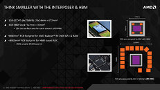
Since the introduction of its Graphics CoreNext architecture in 2012, AMD has been rather laxed in its product development cycle. The company has come out with a new high-end silicon every 18-24 months, and adopted a strategy of cascading re-branding. The introduction of each new high-end silicon would relegate the existing high-end silicon to the performance segment re-branded, and the existing performance-segment silicon to mid-range, re-branded. While the company could lay out its upcoming Radeon R9 series much in the same way, with the introduction of essentially just one new silicon, "Fiji," it could just prove enough for the company. Much like RV770, "Fiji" is about to bring something that could prove to be a very big feature to the consumer graphics market, stacked high-bandwidth memory (HBM).HBM is being promoted as an upcoming memory standard by JEDEC, and AMD will be the first company to build an ASIC implementing it; with SK Hynix being among the first DRAM makers to build silicon for the standard. HBM is being brought in to address a key problem with GDDR5 - it's not being able to keep up with the growing video memory bandwidth demands of upcoming applications and the GPUs being built to drive them. AMD already has the fastest implementation of GDDR5 on its "Hawaii" silicon, which belts out 320 GB/s of memory bandwidth, but to get there, the company is having to use sixteen memory chips. Placed on a PCB, the ASIC along with the 16 memory chips take up quite a bit of real-estate - 110 mm x 90 mm (99 cm²).
GPU makers haven't managed to take clock speeds of GDDR5 above 1752 MHz (real), and the fact that they're having to use other ways to increase effective bandwidth, such as proprietary lossless memory compression, shows that GDDR5 will fetch diminishing returns for new designs from here on, out. With GDDR5 (or any DRAM standard for that matter), power-consumption doesn't follow a linear curve to support increasing clock speeds. Beyond a point, you need a disproportionate amount of power to support increasing clocks. GDDR5 reached that point. This necessitates HBM.
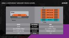
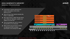
HBM takes a different approach to achieving memory bandwidth than GDDR5. The interface is wider, but with lower clocks (leaving a vast room for future increases in clock speeds). The first generation of HBM, which AMD is implementing on its upcoming high-end graphics cards, pushes just 1 Gbps of data per pin (compared to 7 Gbps on the fastest GDDR5); but features a vast bus width of 1024-bit (compared to just 32-bit per GDDR5 chip). An HBM "chip" is essentially a stack of five dies - a "base die" which holds routing logic, and four DRAM dies, stacked like pancakes (compared to just one DRAM die being bumped out to a BGA package that sits on the PCB, on GDDR5).
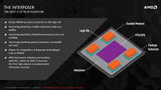
In AMD's implementation of HBM, these "chips" won't be encased into ceramic packages of their own, that sit outside the GPU package, to which it takes intricate wiring along the PCB to reach out to. Instead, HBM chips will be placed right alongside the GPU die, inside the GPU package, on a package substrate AMD calls the "interposer." This is a specially designed substrate layer above the ASIC's own package substrate, which connects the GPU die to the four HBM stacks, with an extremely high density of wiring, that's beyond what conventional multi-layered fiberglass PCBs are capable of. The interposer is perhaps the closest man has come to developing a medulla oblongata.
These stacks, as a result are much closer to the GPU silicon, and the interposer enables extremely high memory bus widths thanks to the density of wiring it can handle. AMD has four such stacks on its upcoming "Fiji" ASIC, resulting in a gargantuan 4096-bit memory bus width. Since HBM pushes lesser data per pin compared to GDDR5, don't expect "Fiji" to have eight times the memory bandwidth as "Hawaii." AMD's flagship Radeon graphics card based on "Fiji" is rumored to feature a memory clock speed of 500 MHz (1 Gbps per pin), which translates in to 512 GB/s of cumulative video memory bandwidth for the GPU, with 128 GB/s per HBM stack. The DRAM voltage is lower, at 1.3V, compared to 1.5V on 7 Gbps GDDR5.
The specifications of the GPU die are constantly being churned up by the rumor mill. Regardless of that, "Fiji" will end up having a lower PCB footprint than "Hawaii." The package will be bigger, but it will no longer be surrounded by memory chips. The PCB look quite different from what we're used to seeing, since the dawn of PC graphics add-in boards. In a way, that's a great thing. AMD retains control over memory, and so its AIB partners can't cheap out with memory chips. We haven't forgotten how some AIBs shortchanged buyers of Radeon R9 290 and R9 290X with cheaper Elpida GDDR5 chips on reference PCBs, even as initial batches (and review samples), came with higher-quality SK Hynix-made ones. Some of the earliest boards with Elpida chips didn't have proper memory timing optimization in the video-BIOS, prompting AIBs to send out BIOS updates. Something like that won't happen with "Fiji," and AIBs are free to cheap out on PCB quality, as the most sensitive wiring (that between the GPU and memory), has now been moved to the GPU package, and its interposer (more quality control in AMD's hands).
So what does this all boil down to? The memory is a more important ingredient in a modern graphics card, than you've been led to believe. The 64-bit computing era is now firmly here, and games are taking advantage of any amount of system- and video-memory you can throw at them. Compound that with DirectX 12, in which the command buffer can take advantage of any number of CPU cores you throw at it, tiled resources, and you're looking at a future that AMD seems to have been preparing for the the past decade (CPUs with a large number of cores, GPUs with extremely high number-crunching parallelism and memory bandwidth). HBM and the way AMD implemented in on its "Fiji" silicon is an important cog in the company's machine. It will offer a brand-new path of bandwidth upscaling through clock speed upscale; and higher energy-efficiency.
It's improbable that AMD would go to such lengths to equip its new high-end silicon, if it wasn't confident of outperforming anything NVIDIA has right now. Likewise, it's improbable that AMD would give a GPU 512 GB/s of memory bandwidth to toy with, if it lacked the chops (number-crunching muscle) to deal with such amount of memory. And this, is what makes "Fiji" a chip to look out for. AMD is expected to tease graphics cards based on "Fiji" at either Computex or E3, with a product launch within June. Let the battle between the Titans and the House of Zeus begin.

29 Comments on AMD "Fiji" HBM Implementation Detailed
I suppose R7s will still get GDDR5 but I hope there's at least an R9 380X with HBM.
Would like to see an APU (BGA i presume) with a large interposer to house CPU/GPU/HBM.
And all of that on a small form factor board.
Also, i thought that free-sync was dependent on the monitor's support, and all Graphics CoreNext based cards are technically Free-Sync compatible. Guess not.
In all seriousness though I'm looking forward to much smaller pcbs and waterblocks. If we can get some CPUs with HBM we might even get itx form factor dual GPU setups. :clap:
(It's weird that Nvidia being the one making the more money atm is the one making the fewer chip: 4 vs at least 10 for amd...)
Guys, come on!
If that was the case, ATI could simply make the cards "artificially" bigger to accomodate a larger blower.
One must note, however, that ever since the hotter-than-the-sun GTX480 was released in 2009, ATI has succesfully claimed the "hottest" product crown. It will be great to see them back on the game again.
Hope the same happens with AMD CPUs as well.
This would effectively double the surface area used for cooling.
I hope AMD have spent enough time validating this. the links are really fragile, and if they get hot. think Xbox 360 issues 1 billion dollars in writeoffs from warranty! if its not 100% sorted
And that's what baffles me with AMD's Radeon product lines. There are TOO MANY of them. Bunch of Rx editions and then those are granulated down to bunch of series and then down to special models and versions. Totally unnecessary, confusing and overwhelming for costumers.
Why not have just R9 and place 4-5 well placed models here. Simulated naming for the new R9-300 series:
R9-320 2GB (budget)
R9-350 2GB (low end)
R9-370 3GB (mid range)
R9-380 4GB (high end)
R9-390 4GB/8GB* (premium-enthusiast)
*depending on how HBM can be implemented currently
No X versions, no LE crap versions, no various memory configurations, no R5 and R7 unless if you want to separate lets say mobile chips from desktops that way. When you give people a good argument why they should pay few bucks more, they will do so. But if you're having hard time justifying why every iteration of a card in between costs X for function Y, you just confuse costumers and make them walk away because they have to "rethink". And everyone who has to rethink is more likely to buy something from competition.
I don't know, I don't have a science degree in space marketing and a 6 figure yearly income and I get this. But companies just go with heads straight through the walls. Go figure...
what happened was this mess with TSMC, lack of resources, shopping time of the year, OEMs needing new/more numbers.... so you end up with rebrands, mixed generations, & stop-gap solutions
you messed up with your Rx, R9 is high end, R7 is midrange, R5 is low end (this is so consumers get an idea of performance level.... even though it's a bit redundant cuz a higher numbered 280 is obviously better than 260, but i guess it doesnt communicate which third of performance it is cuz consumers are idiots that need their hands held all the time instead of using a 1-10 scale (wow it took me this long to realize it's based on intel's i3, i5, i7))
i'm actually not sure why you say there are so many products, nvidia has the same issue when there are TI editions & especially with mobile
the product stack is pretty normal on launch, with a few random appearances months or years later like the 5830 or 285
hmm maybe i should imagine my own (gaming, not workstation) stack, which btw needs price points:
$53 - 310 - are you sure you want to permanently delete this file?
$60 - 320 - i dont even know what i would do around here, rebadge? keep cutting tiny gpus? try to engineer low power efficiency for practice?
$70 - 330 - 9fps - borderline worse than an APU, probably should be required to playback 4k30 video
$85 - 340 - 12fps - maybe slowed & cut low end gpu... i hate low end, people cant wait a week to save up a couple bills? it's not like faster last gen cards are obsolete, buy those at this price instead
$100 - 350 - 15fps - upper low end gpu, will struggle if MSAA is used in 1080p
$125 - 360 - 19fps - slowed & cut mid gpu
$150 - 365 - 23fps - mid gpu that should handle 1080p without constantly being limited by ROPs or bandwidth, but eye candy will slow it down fast
$175 - 370 - 27fps - slowed & cut upper mid tier gpu
$200 - 375 - 32fps - uncut upper mid tier gpu that performs half or physically contains mostly half of the high end gpu
$250 - 380 - 38fps - slowed & cut second tier gpu
$300 - 385 - 46fps - uncut second tier gpu (maybe it lacks all the compute parts like 7870 did but still has more parts for raster rendering)
$350 - 390 - 53fps - slowed & cut big gpu
$450 - 395 - 60fps - full speed uncut big gpu, the absolute best single gpu (mass produced, not workstation, not custom or limited/specialized run such as some server compute card)
$750 - 390x2 - 4k 45fps - cut or slightly slowed dual big gpu (x2 because naming a dual gpu without a dual number is STUPID & unclear, ever since the 290+5970...)
$950 - 395x2 - 4k 55fps - water cooled full speed dual uncut big gpu
there is a glaring hole in my idea... it's quite similar to the 7 series, i actually do wonder what would happen if they made a really high end gpu based on the 7870's principles, as in, instead of adding compute capability, to just make a fat one that is only good in games... but this costs so much money for no gain, especially when you're making an ecosystem of gpu accelerated computing such as photoshop, video encoding, etc
inb4 the million custom editions that AIBs make, especially the OC ones that cost up to the next product that might ironically perform worse than that next product
here's a fun potential fact: titan -> titan z (titans, it's dual) -> titan x (titan next, it's the sequel)
EDIT: changed 390x2 price from original $850 that was based on limitations of air cooling nearly 300 watts
However don't expect the 380X to have HBM. They need to use as much of it as they can on the 390 series. Actually the 380X is rumored to be "Enhanced Hawaii" with 8GB of GDDR5 - and that at least still sounds great.