News Posts matching #Hynix

Return to Keyword Browsing

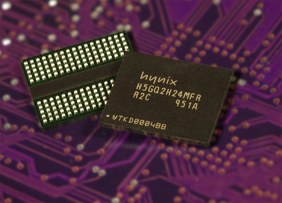
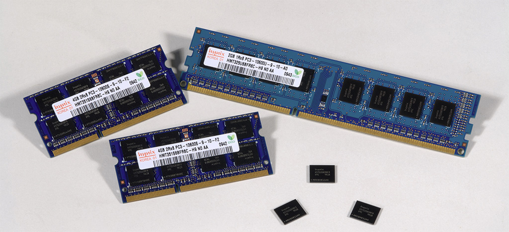
EU Slaps Chip Vendors with Penalties for Price-Fixing

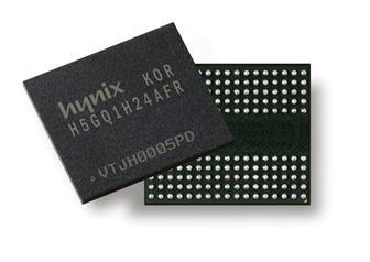
As many as nine major chip vendors were fined a total of 331 million Euros (US $404.2 million) for participating in illegal price-fixing activities, by the European Union authorities. These include Samsung, Hynix, Nanya, Elpida, Infineon, NEC, Toshiba, Hitachi, and Mitsubishi. A 10th company in this price-fixing cartel was Micron Technology, which escaped the fine for exposing the malpractice to the EU authorities. Of these Samsung was given the single biggest fine of 146 million Euros, followed by Infineon at 57 million Euros. The fines were reduced by 10% because all companies extended cooperation in the investigations.

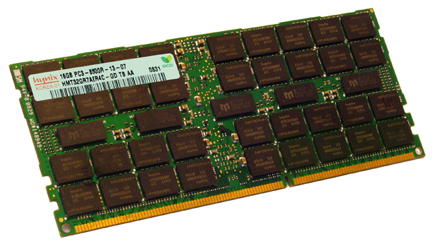
The price-fixing cartel mostly involved bad trade of DRAM chips, and was active between 1998 and 2002, operating with a network of contacts which secretly exchanged pricing information. They colluded to fix prices of DRAM chips sold to major PC and server manufacturers. Investigations in the scam began in 2002 when Micron blew the whistle on the cartel. "By acknowledging their participation in a cartel the companies have allowed the Commission to bring this long-running investigation to a close and to free up resources to investigate other suspected cartels," said EU's Competition Commissioner, Joaquin Almunia. "As the procedure is applied to new cases it is expected to speed up investigations significantly," he added.

Hynix Introduces World's First 40 nm Class 2 Gb GDDR5 DRAM

Hynix Semiconductor Inc., today announced the industry's first 2 Gb (Gigabit) GDDR5 called H5GQ2H24MFR-R2C using its leading-edge 40nm class process technology.

The newly developed GDDR5 is the fastest and highest density graphics memory available in the market. It operates at 7 Gbps (Gigabit per second) bandwidth and processes up to 28 GB/s (Gigabytes per second) with a 32-bit I/O. In addition to its fastest speed and highest density, it is also designed to minimize power consumption with 1.35V operation voltage. It is an 'eco-friendly' device which reduces energy consumption by 20% over the preceding memory solutions using 50nm class technology.

Hynix Announces the Intel Validation of 40nm Class 2Gb DDR3 Products

Hynix Semiconductor, Inc. has announced the Intel validation of 2Gb (Gigabit) DDR3 DRAM using 40nm class process technology.

Hynix's newly validated products are 2Gb DDR3 SDRAM component, 4GB (Gigabyte) DDR3 SODIMM (Small Outline Dual In-line Memory Module) and 2GB DDR3 UDIMM (Un-buffered Dual In-line Memory Module) at the operating speed of 1333MHz with 1.5V power supply.

The products can offer the maximum data transfer speed of 1867MHz with 16-bit I/O and 3.7GB/s (Gigabytes per second) bandwidth. The productivity of Hynix's 40nm class 2Gb DDR3 is increased by more than 60% over 50nm class process technology.

Hynix Introduces the Second Generation 1Gb DDR3

Hynix Semiconductor, Inc. has announced the second generation 1Gb (Gigabits) DDR3 using 54nm process technology. Hynix's new 1Gb DDR3, offered in x4 (H5TQ1G43TFR) and x8 (H5TQ1G83TFR) organizations, has innovative design modifications that significantly reduce power consumption of the device.

The new product operates at 1.5V (volts) power supply as the existing 1Gb DDR3 product and further reduces power consumption by 30% over the existing one. This second generation product is the highest performing memory in the industry among 1Gb density category which is the mainstream of the products. According to the iSuppli, a market research firm, the portion of the world wide 1Gb DDR3 is currently estimated to be 87%. The iSuppli estimates that higher densities will become the mainstream when it is expected to account for more than 50% in 2011.

Zotac Designs Shorter GeForce GTX 260 Accelerator

Zotac's design team is at it again, releasing a newer graphics card design based on the NVIDIA GeForce GTX 260 GPU. This one, concentrates on making the card shorter, lengthwise. The shorter graphics card also makes do with just one 8-pin PCI-Express power connector. The PCB length is lopped from the typical 26.5 cm to 23 cm, making it easier to fin in smaller cases. With the PCB compact, several heat-producing components are moved closer to each other, making it easier to cool with a smaller common cooler base plate.

Hynix Introduces 4Gb Mobile DDR SDRAM Supported on Intel's Moorestown Platform

Hynix Semiconductor, Inc. announced the 4Gb (Gigabits) mobile DDR SDRAM is now supported on Intel's 'Moorestown' platform for MID (Mobile Internet Device) applications.

This high density memory device packs twice the storage capacity over current 2Gb mobile memory solutions and is offered in small form factor packages such as MCP (Multi Chip Package) and PoP(Package on Package). It boasts maximum operating speed of 400Mbps (Megabits per second), processing up to 1.6GB (Gigabytes) of data per second with a 32-bit I/O.

Hynix, LG, Samsung Electronics and Silicon Image Join to Develop Serial Port Memory

Hynix Semiconductor, LG Electronics , Samsung Electronics, and Silicon Image, today announced the formation of an industry consortium that promotes Serial Port Memory Technology (SPMT) for broad market adoption as an industry standard. As the first-of-its-kind memory specification for dynamic random access memory (DRAM), SPMT will initially target the mobile handset market, enabling a new generation of devices capable of running highly data intensive, media-rich applications while at the same time extending battery life.

Hynix, Numonyx and Phison Join to Develop NAND Memory System Solutions

Hynix Semiconductor Inc, Numonyx B.V. and Phison Electronics Corp. today announced that they have signed a collaboration agreement to jointly develop controllers for the next generation of managed-NAND solutions based on the newly released JEDEC eMMC 4.4 industry specification. The collaboration is expected to speed the delivery of the industry's most advanced eMMC specification available, helping to manage and simplify high-capacity storage requirements and improve the overall system-level performance of wireless and embedded applications.
Under this agreement, Phison, Hynix and Numonyx will leverage their respective competencies to develop controllers used in combination with a variety of NAND flash products. Phison will exclusively supply the jointly developed controllers to Hynix and Numonyx, which will enhance their respective NAND flash memory solutions portfolio.

Hynix Announces High Speed, Low Power 50nm-class DDR2 DRAM

Hynix Semiconductor, Inc. announced that it has developed the world's first mobile 1Gb DDR2 DRAM using 54nm process technology. By successfully developing a 50nm-class process, Hynix has overcome the challenge of producing mobile DRAMs with both high speed and low power consumption features.

This device is offered at a maximum speed of 1066MHz, and with 32-bit I/O, boasts bandwidth of 4.26GB/s(Giga byte per second) on a single channel device and 8.52GB/s on a dual channel. Hynix's 'One Chip Solution' design, offers the customer flexible options with 2-bit or 4-bit prefetch, and 16 or 32-bit I/O on a single chip. Additionally, Hynix's new mobile DDR2 is an eco-friendly device since it consumes only 50% of power compared to the previous generation mobile DDR, and 30% compared to standard DDR2 DRAM.

Hynix Announces Validation of the World’s First 8 GB 2-Rank DDR3 R-DIMM

Hynix Semiconductor today announced the validation of the HMT31GR7AUP4C, the world's first MetaRAM based 8 GB 2-rank DDR3 RDIMM, on Intel's Nehalem CPU based Tylersburg-EP platform
When fully populated with 3 DIMMs per channel, the Hynix 8 GB RDIMM operates at 1066 MHz speed. Competing industry standard modules exhibit performance degradation to 800 MHz when operating under full load. The Hynix 8 GB DDR3 RDIMM enables a maximum capacity of 144 GB operating at 1066 MHz in a dual processor Tylersburg-EP platform, not possible with industry standard DIMMs.

Zotac Expands its GTX 285 Lineup, Uses Accelero Xtreme Cooler

Zotac has yet another GeForce GTX 285 SKU in the making. This time, it plans to use its own-designed GTX 285 PCB with an Arctic Cooling Accelero Xtreme GPU cooler. Zotac isn't using the entire kit, as the NVIO2 and VRM heatsinks aren't compatible with this PCB design. Other manufacturers using this cooler for similar graphics cards include Galaxy, which uses it for its GTX 285 2 GB, and Inno3D, which uses the entire kit for its GTX 280 accelerator.

With the new PCB design, Zotac rearranged the card's VRM area. The design differs from another PCB design for the GTX 285 Zotac designed earlier (read here). The card uses 6 vGPU + 3 vMem power phases. Ferrite-core chokes are made use of, and an extra vGPU phase has been added for redundancy and stability (angled chokes next to the power connectors, pictured below). 1 GB memory across a 512-bit interface is present, with the company making use of Hynix N3C 0.77 ns GDDR3 chips. The clock speeds on this card adhere to NVIDIA's specifications: 648/1476/1242 MHz (core/shader/memory). The SKU is almost ready to be announced.

Rambus and Hynix Agree on Damages and Terms for Compulsory License

Rambus today announced that it has agreed in principle to terms for a compulsory license with Hynix Semiconductor (000660.KS) for SDR SDRAM and DDR SDRAM memory products. The parties have agreed to royalty rates of 1% for SDR SDRAM and 4.25% for DDR SDRAM memory devices for net sales after January 31, 2009 and before April 18, 2010. The latter rate applies to DDR, DDR2, DDR3, GDDR, GDDR2 and GDDR3 SDRAM devices, as well as DDR SGRAM devices. In addition, a proposed final judgment of $349M in damages, plus pre-judgment interest of approximately $48M has been submitted to the U.S. District Court for the Northern District of California. The final amount of pre-judgment interest depends on the date final judgment is entered. Damages and royalty rates are limited to U.S. infringements.

GIGABYTE Releases Ultra Durable VGA (UDV) Technology

GIGABYTE Technology Co. LTD., a leading manufacturer of motherboards and graphics cards, today launched the latest GIGABYTE unique technology: Ultra Durable VGA. GIGABYTE latest innovative technology-Ultra Durable VGA features 2 oz copper PCB board, Samsung/Hynix memory, Japanese solid capacitor, Ferrite Core Chokes, and Low RDS (on) MOSFET to deliver incredibly low GPU temperature, unrivaled overclocking capability, low power switching loss, and guaranteed longer life. Compared with traditional graphics accelerators, Ultra Durable VGA graphics accelerators can lower GPU temperature by 5%~10%, lower power switching loss by 10%~30%, and increase overclocking capability by 10%~30%. GIGABYTE Ultra Durable VGA graphics accelerators can provide truly both "high-performanced" and "green" graphic card resolutions.

Court Grants Rambus Supplemental Damages in Hynix Case

Rambus Inc., one of the world's premier technology licensing companies specializing in high-speed memory architectures, today announced that the U.S. District Court for the Northern District of California has granted its request for supplemental damages following an earlier jury verdict finding nine Rambus patents valid and infringed by Hynix SDRAM products. According to the order, Hynix is to pay Rambus royalties of 1% for SDR SDRAM products and 4.25% for DDR SDRAM products made, used, or sold in the United States after December 31, 2005. DDR SDRAM products include DDR SDRAM, DDR2 SDRAM, DDR3 SDRAM, GDDR SDRAM, GDDR2 SDRAM, GDDR3 SDRAM, and DDR SGRAM. These supplemental damages are in addition to those previously awarded in the amount of $133M for Hynix's infringement through December 31, 2005.

Hynix 40nm 1Gb DDR3 DRAM Chip to Enter Production in 3Q'09

Hynix forms one of the top-tier DRAM manufacturers. On Sunday, the company made it official that its new 1 Gb (128 MB) DDR3 memory chip built on the new 40 nm silicon fabrication process, will enter mass production by the third quarter, and be available to manufacturers soon after. The chip (model: H5TQ1G83CFR) operates with a top-speed of 2,133 Mbps, at a wide range of voltage.

Using the three-dimensional transistor technology, the company has stepped-up productivity by more than 50% over its current DRAM chips built on the 50 nm process. The new technology is said to minimize electric leakages and reduces overall power consumption of the DRAM chip. The new 1Gb memory chip meets Intel's DDR3 DRAM specification compliance and the memory module will be examined for certification by Intel.

Hynix Semiconductor Develops the World’s First 2Gb Mobile DRAM

Hynix Semiconductor announced it has developed the world's first 2Gigabit mobile DRAM using 54nm process technology. This product provides twice as much storage capacity over current 1Gb mobile solution which has been the highest density offered among the mobile DRAM products in MCP(Multi Chip Package), PoP(Package on Package) platform. It boasts maximum operating speed of 400Mbps(Megabits per second) at 1.2V power supply and processes up to 1.6 Gigabytes of data per second with a 32-bit I/O. Moreover, the new product consumes less power than existing memory solutions.

Hynix 7GT/s GDDR5 Chip to Make it to Major SKUs, R700 Included

Sources in the industry point out that the 7 GT/s GDDR5 memory chip made by Hynix (model: H5GQ1H24AFR), which was announced earlier in this week, would make it to several major graphics board SKUs by both AMD and NVIDIA. The two companies have chosen TSMC and its 40nm fabrication process as the foundry partner for their upcoming 40nm graphics processors, namely AMD RV870 and NVIDIA GT212.

Both these chips would feature GDDR5 memory bus capabilities, and there are indications of the 7 GT/s DRAM chip being incorporated into graphics boards based on these GPUs. Additionally, there is also word that AMD will be using the said DRAM chip in its current flagship graphics card, the Radeon HD 4870 X2 in the near future. Both AMD and NVIDIA are expected to have taped out their 40nm GPU designs within Q1, 2009.

Hynix Rolls-out 7 GT/s GDDR5 Memory Chip

DRAM major, Hynix has announced the depelopment of 7 GT/s GDDR5 memory chips for use by the visual-computing industry. These chips are built on the company's 54nm silicon fabrication technology.

The 1 Gb (128 MB) chips labelled H5GQ1H24AFR operate at the fastest speeds so far: 7 Gbps (or GT/s), which is a 40% boost in speeds compared to the older 5 GT/s chips already in production. The chip handles up to 28 GB of data per second across a 32-bit wide interface. The incorporation of new fab. processes also means reduced power consumption at 1.35V power supply. The JEDEC-standard 1Gb GDDR5 graphics DRAM chip targets high-end applications such as game consoles and graphics cards. The company will commence volume production in the first half of 2009.

Hynix Demonstrates World's First 16GB DDR3 2-Rank R-DIMM Memory at IDF

Among the other hardware demonstrated at IDF, Hynix Semiconductor also made a shocking release of what's believed to be the world's first 16GB 2-Rank R-DIMM. Using MetaRAM's new DDR3 technology, Hynix's new 16GB (HMT32GR7AER4C-GD) and 8GB (HMT31GR7AER4C-GC) 2-rank DIMMs can triple DDR3 memory capacity in today's servers and workstations. DDR3 MetaRAM is similar to the previous generation of DDR2 technology that enables significantly more memory in a server. An added benefit of the DDR3 MetaRAM technology is that enables larger memory capacity without negatively impacting the operating frequency of the DDR3 memory channel. It is the only technology that has been demonstrated to run 24GB of DDR3 SDRAM in a channel at 1066 million transactions per-second (MT/s). Using 3 of 16GB DIMM, users can achieve 48GB per channel running at 1066 MT/s, while other competing solutions max out at 16GB per channel at 1066MT/s. Later on during the Intel Developer Forum (IDF) in San Francisco Intel will demonstrate a server with 160GB (10 slots) of Hynix's DDR3 R-DIMMs.

Numonyx and Hynix Partnership to Introduce New, Innovative NAND Flash Products

Hynix Semiconductor and Numonyx B.V. today announced a five-year agreement to expand its joint development programs for the fast-growing NAND flash memory segment. The companies will broaden NAND product lines and bring future product and technology innovations designed to address challenges facing NAND technology over the next five years.

Memory Configurations of RV730 and RV710 Come to Light

Admidst the a virtual arms race between the two giants of the discrete graphics industry, information trickles about the memory configurations that the mid-range RV730 (Radeon HD4650 / HD4670) and entry-level RV710 (Radeon HD4450 / HD4470) come in.

NordicHardware reports that two different GDDR3 memory configurations could be seen with RV710. Both configurations operate at 800MHz, but the density varies from 512MB Hynix memory to 1024MB Samsung chips. This points to that the HD4450 and HD4470 models will be separated by GPU clock. RV730 offers a bit more variation with three different clock frequencies and two different densities. One 700MHz 512MB model, and two 900MHz models, of which one sports 512MB Hynix memory and one sports 1024MB Samsung chips. And finally, there is one model with 512MB Hynix memory operating at 1000MHz. It is assumed that the Radeon HD 4650 is the 700MHz cards, while the 4670 model is represented by the three remaining cards.

Seagate Still Sourcing NAND Flash

With announcements coming in from of rolling out Solid State Drives (SSD) and that it would become a prominent player in the SSD business, Seagate is still in requirement of trade relationships with a NAND Flash manufacturer, add to that it doesn't have production facilities of its own.

This has gotten analysts to speculate on where Seagate will source its chips from, a possibility being buying Intel's share of the Intel-Micron JV. Such a buy-out would set Seagate back by close to $1 bn. Another possibility would be to acquire SanDisk or Hynix (Hyundai) which focus on making entry-level solid state drives, but are a major players in the overall NAND flash market. If it will be SanDisk, Hynix or any other flash maker remains to be seen, but it wouldn't come as a surprise if Seagate announces the acquisition of a flash company soon.

Hynix and ProMOS Sign Agreement to Strengthen Long-term Strategic Alliance

Hynix Semiconductor and ProMOS Technologies today announced the signing of the Amendment to strengthen their existing strategic alliance. According to the Amendment, Hynix licenses to ProMOS 50 nanometer-class DRAM stack process technology, while ProMOS offers to Hynix such DRAM products from its 300mm fab capacity. To achieve timely technology transfer, Hynix plans to commence the government filing process immediately. Additionally, Hynix plans to cooperate with some financial investors to buy 8%-10% portion of shares in ProMOS through private placement to strengthen their long-term cooperation relationship.

Hynix Developed the World’s Fastest 1Gb Low-Power DDR2

Hynix Semiconductor today introduced the world's first and fastest 1 Gigabite mobile LPDDR2. This product meets JEDEC standard and is expected to lead international LPDDR2 standard. 1Gb LPDDR, Low Power DDR2, is built on the Company's leading edge 66nm process technology. It boasts maximum operating speed of 800Mbps at 1.2V power supply. It consumes less power but operates at a faster speed than mobile DDR. With the fastest speed and small form factor package of 9mm x 12mm,, it is designed to meet the needs of a wide range of mobile applications which demand high memory density and fast operating speed features. This new product has function of Hynix's 'One Chip Solutions' and it allows Hynix the flexibility of offering wire bonded options to meet the specific needs of the customer by combining SDRAM/DDR DRAM interfaces, and x16/x32 organizations on a single chip. Hynix plans to start mass production of LPDDR2 in the fourth quarter of this year to meet the increasing demand for high performance mobile applications.
Return to Keyword Browsing
Jul 3rd, 2025 21:11 CDT change timezone

New Forum Posts

Popular Reviews

TPU on YouTube

Controversial News Posts