News Posts matching #HyperTransport

Return to Keyword Browsing

Chinese Loongson 3D5000 Features 32 Cores and is 4x Faster Than the Average Arm Chip

Amid the push for technology independence, Chinese companies are pushing out more products to satisfy the need for the rapidly soaring demand for domestic data processing silicon. Today, we have information that Chinese Loongson has launched a 3D5000 CPU with as many as 32 cores. Utilizing chiplet technology, the 3D5000 represents a combination of two 16-core 3C5000 processors based on LA464 cores, based on LoongArch ISA that follows the combination of RISC and MIPS ISA design principles. The new chip features 64 MB of L3 cache, supports eight-channel DDR4-3200 ECC memory achieving 50 GB/s, and has five HyperTransport (HT) 3.0 interfaces. The TDP configuration of the chip is officially 300 Watts; however, normal operation is usually at around 150 Watts, with LA464 cores running at 2 GHz.

Scaling of the new chip goes beyond the chiplet, and pours over into system, as 3D5000 supports 2P and 4P configurations, where a single motherboard can become a system of up to 128 cores. To connect them, Loongson uses a 7A2000 bridge chip that is reportedly 400% faster than the previous solution, although we have no information about the last chip bridge. Based on the LGA-4129 package, the chip size is 75.4x58.5×6.5 mm. Regarding performance, Loongson compares it to the average Arm chip that goes into smartphones and claims that its designs are up to four times faster. In SPEC2006, performance reaches 425 points, while maintaining a single TeraFLOP at dual-precision 64-bit format. On the other hand, the processor was built for security, as the chip has a custom hardware-baked security to prevent Spectre and Meltdown, has an on-package Trusted Platform Module (TPM), and has a secret China-made security algorithm with an embedded custom security module that does encryption and decryption at 5 Gbps.

Intel Announces New Mesh Interconnect For Xeon Scalable, Skylake-X Processors

Intel's "Xeon Scalable" lineup is designed to compete directly with AMD's Naples platform. Naples, a core-laden, high performance server platform that relies deeply on linking multiple core complexes together via AMD's own HyperTransport derived Infinity Fabric Interconnect has given intel some challenges in terms of how to structure its own high-core count family of devices. This has led to a new mesh-based interconnect technology from Intel.

AMD Ryzen Infinity Fabric Ticks at Memory Speed

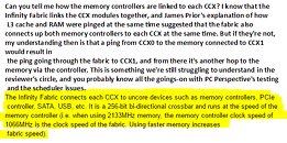
Memory clock speeds will go a long way in improving the performance of an AMD Ryzen processor, according to new information by the company, which reveals that Infinity Fabric, the high-bandwidth interconnect used to connect the two quad-core complexes (CCXs) on 6-core and 8-core Ryzen processors with other uncore components, such as the PCIe root-complex, and the integrated southbridge; is synced with the memory clock. AMD made this revelation in a response to a question posed by Reddit user CataclysmZA.

Infinity Fabric, a successor to HyperTransport, is AMD's latest interconnect technology that connects the various components on the Ryzen "Summit Ridge" processor, and on the upcoming "Vega" GPU family. According to AMD, it is a 256-bit wide bi-directional crossbar. Think of it as town-square for the chip, where tagged data and instructions change hands between the various components. Within the CCX, the L3 cache performs some inter-core connectivity. The speed of the Infinity Fabric crossbar on a "Summit Ridge" Ryzen processor is determined by the memory clock. When paired with DDR4-2133 memory, for example, the crossbar ticks at 1066 MHz (SDR, actual clock). Using faster memory, according to AMD, hence has a direct impact on the bandwidth of this interconnect.

AMD Talks Zen 3, "Raven Ridge," and More at Reddit AMA

AMD, at its post-Ryzen 7 launch Reddit AMA, disclosed some juicy details about its other upcoming socket AM4 chips, beginning with the rest of the Ryzen 5 and Ryzen 3 "Summit Ridge" processor roll-out, and a little bit about its 8th generation socket AM4 APU, codenamed "Raven Ridge." To begin with, AMD CEO Lisa Su stated that "Raven Ridge" will also be sold under the Ryzen brand. This would mark a departure from the less-than-stellar A-series branding for its performance APUs. "Raven Ridge" likely combines a "Zen" quad-core CPU complex (CCX) with an integrated GPU based on one of AMD's newer GPU architectures (either "Polaris" or "Vega").

The range-topping Ryzen 7 series will lead the company's lineup throughout Q1, with six-core and quad-core Ryzen 5 and Ryzen 3 series launches being scheduled for later this year. Our older reports pinned Ryzen 5 series rollout for Q2, and Ryzen 3 series for the second half of 2017. This is likely also when the company rolls out "Raven Ridge" initially as mobile Ryzen products (BGA packages, which will likely also be used in AIOs), and later as desktop socket AM4 parts.

NVIDIA "Pascal" GP100 Silicon Detailed

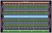
The upcoming "Pascal" GPU architecture from NVIDIA is shaping up to be a pixel-crunching monstrosity. Introduced as more of a number-cruncher in its Tesla P100 unveil at GTC 2016, we got our hands on the block diagram of the "GP100" silicon which drives it. To begin with, the GP100 is a multi-chip module, much like AMD's "Fiji," consisting of a large GPU die, four memory-stacks, and silicon wafer (interposer) acting as substrate for the GPU and memory stacks, letting NVIDIA drive microscopic wires between the two. The GP100 features a 4096-bit wide HBM2 memory interface, with typical memory bandwidths of up to 1 TB/s. On the P100, the memory ticks at 720 GB/s.

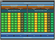
At its most top-level hierarchy, the GP100 is structured much like other NVIDIA GPUs, with the exception of two key interfaces - bus and memory. A PCI-Express gen 3.0 x16 host interface connects the GPU to your system, the GigaThread Engine distributes workload between six graphics processing clusters (GPCs). Eight memory controllers make up the 4096-bit wide HBM2 memory interface, and a new "High-speed Hub" component, wires out four NVLink ports. At this point it's not known if each port has a throughput of 80 GB/s (per-direction), or all four ports put together.

More AMD Socket AM4 Technical Details Emerge

More details of AMD's upcoming common socket for both its desktop APUs and high-end CPUs emerged from a recent article by Italian tech-site Bits-n-Chips. To begin with, AM4 will be an µOPGA (pin-grid array), in which the pins will continue to be located on the processor package, and contact points on the socket. The package will be square, and 40 mm in length, making it about as big as a current socket FM2+ package. It will have a pin-count of 1,331 pins, a big increase from the 942 pins of AM3+, and 906 pins of FM2+. AMD could continue to develop LGA sockets for its multi-socket capable Opteron processors based on the "Zen" architecture.
The AM4 platform layout will be functionally closer to that of the FM2+ than the AM3+. Besides the integrated memory controller, the northbridge will be entirely located on the processor die; and so the HyperTransport main system bus will be wired internally. Besides hundreds of electrical pins, the AM4 pin-map will consist of memory I/O, integrated graphics I/O, PCI-Express, and the chipset bus; besides other low-level system I/O interfaces. The memory controller on some of the first AM4 chips, such as "Summit Ridge," will natively support DDR4-2400 MHz, and DDR4-2933 MHz through overclocking.
AMD Readies Two New Performance-segment FX Processors

AMD is preparing to expand its performance-segment socket AM3+ processor lineup, steering clear of the 220W TDP of its FX-9000 series. The two chips are the FX-8370, and the FX-8370E. The FX-8370 will likely replace the FX-8350 around the $180 mark; while the FX-8370E will be its energy-efficient variant. Both chips offer clock speeds of 4.10 GHz, with 4.30 GHz TurboCore frequencies. While the FX-8370 has a rated TDP of 125W, the FX-8370E features 95W, without a reduction in clock speeds. The FX-8370E could hence come at a slight premium.

Both the FX-8370 and FX-8370E are eight-core processors based on the 32 nm "Vishera" silicon, featuring four "Piledriver" CPU modules that have 2 MB of L2 cache each, and 8 MB of L3 cache shared between the four modules. The chips feature dual-channel DDR3 integrated memory controllers, with native support for DDR3-1866 MHz, and 5.2 GT/s HyperTransport 3.1 system bus. Instruction-sets include AVX, AES, SSE4.2, FMA3, and XOP. The chips will run on all existing socket AM3+ motherboards, with some needing BIOS updates.

AMD Readies 16-core Processors with Full Uncore

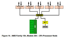
AMD released developer documentation for a new processor it's working on, and the way it's worded describes a chip with 8 modules, working out to 16 cores, on a single piece of silicon, referred to as Family 15h Models 30h - 3fh. This is not to be confused with the company's Opteron 6300-series "Abu Dhabi" chips, which are multi-chip modules of two 8-core dies, in the G34 package.

What's more, unlike the current "Abu Dhabi" and "Seoul" chips, the new silicon features a full-fledged uncore, complete with a PCI-Express gen 3.0 root complex that's integrated into the processor die. In what's more proof that it's a single die with 8 modules and not an MCM of two dies with 4 modules each, the document describes the die as featuring four HyperTransport links; letting it pair with four other processors in 4P multi-socket configurations. Such systems would feature a total core count of 64. There's no clarity on which exact micro-architecture the CPU modules are based on. Without doubt, AMD is designing this chip for its Opteron enterprise product stack, but it should also give us a glimmer of hope that AMD could continue to serve up high-performance client CPU, only ones that can't be based on socket AM3+.

ASRock Fatal1ty 990FX Killer Detailed

Here's the first detailed body-shot of ASRock Fatal1ty 990FX Killer, which was teased by the company earlier today, and which could end up being one of the most feature-rich socket AM3+ motherboards, if the end is neigh for AM3+. Designed for gaming PCs with up to two graphics cards, although it features three long x16 slots, the Fatal1ty 990FX Killer is a full-size ATX motherboard. It's design appears to be more gamer-centric than overclocker-centric. It draws power from 24-pin ATX and 8-pin EPS connectors, with an optional 4-pin Molex connection to stabilize power to add-on cards; and conditions it for the AM3+ CPU using a 10-phase VRM that's cooled by an heatsink that's independent from that which cools the AMD 990FX northbridge (i.e. no heat-pipe linking the two). The AM3+ CPU socket is wired to four DDR3 DIMM slots, which support up to 64 GB of dual-channel DDR3-2400 MHz memory; and to the 990FX northbridge over a 5.2 GT/s HyperTransport link.

The AMD 990FX chipset puts out two PCI-Express 2.0 x16 slots, the third slot is electrical PCI-Express 2.0 x4, and possibly wired to the SB950 southbridge. The southbridge handles five internal SATA 6 Gb/s ports, the sixth port is wired out as eSATA. The Fatal1ty 990FX Killer, as teased this morning, is among the first motherboards to feature an M.2 slot, extended out of a PCI-Express link. PCIe SSDs tend to be faster, as more interface bandwith is on tap. As many as six USB 3.0 ports are on offer, of which one switches between header and internal type-1 port (for those tuck-away software license keys) all of which are driven by third-party controllers. Wired networking is care of a Killer E2200 network controller, that's optimized for gaming. The board features 7.1-channel HD audio, with a high SNR CODEC, PCB ground-layer isolation (to prevent electrical noise), and an EMI shield for the CODEC; which ASRock collectively labels "Purity Sound." The board is driven by AMI UEFI BIOS, with full support for Windows 8 Secure Boot.

AMD Announces Opteron 4300 and 3300 Series Processors

AMD today unveiled nine new mid-range and entry-level AMD Opteron 4300 Series and 3300 Series server processors increasing performance per watt versus the previous generation to maximize compute capabilities in power-constrained environments1, while delivering outstanding value to cloud providers and web hosts. The AMD Opteron 3300 Series processors provide enterprise-class features in a low power envelope at a desktop processor price, making it ideal for web hosts and small- and medium-sized businesses.

The AMD Opteron 4300 Series processors offer up to 15 percent better performance versus the prior generation, based on SPECint benchmark results2. And SPECpower results show up to a 24 percent improvement in performance per watt. As with the AMD Opteron 6300 Series processors, these are socket compatible with the previous generation processor, providing an effortless upgrade path for customers.

Haswell-ULT Processors Could Use 24 MHz BClk, New C-States, and MCM to Cut Power Draw

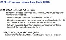
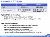
Going into 2013, Intel's tough balancing act between keeping a low power/thermal envelope, and advancing performance, all while staying on the 22 nm silicon fab process, will be care of its Core "Haswell-ULT" processor. The chip will feature some radical changes to traditional Intel processor design, which will help it achieve its design goals. According to a deck of leaked slides scored by Expreview, Intel plans to use additional C-states that drop the processor's base clock, and redesign the processor package to accommodate the PCH silicon, reducing the board footprint.

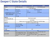
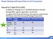
To begin with, Haswell-ULT will be designed to support 24 MHz base clock speed, which running in "deep" energy-saving idle states. Modern processors with FSB replacement interconnect technologies such as QuickPath Interconnect and HyperTransport need a base clock to time other components on the processor, and for low-level communications, while a bulk of the data is transported by the primary interconnect. Intel found a way to turn off the 100 MHz base clock signal (which is also used to time the PCI-Express root complex and integrated graphics core), and replace it with a 24 MHz clock, when the processor is idling. As the processor returns to lower (more active) C-states, the 100 MHz base clock is reapplied. The 24 MHz base clock is activated by three new power states, C8, C9, and C10, introduced by Haswell-ULT. The third slide below details what happens to the various components in the new C-states.

AMD Launches the Opteron 6300 Series Server Processors

AMD today unveiled its new AMD Opteron 6300 Series server processors based on its next-generation "Piledriver" core architecture. The new AMD Opteron processors deliver superior performance and scalability for virtualized server platforms that are central to private and public cloud deployments, big data systems and high-performance computing (HPC) clusters. The AMD Opteron 6300 Series processors strike the ultimate balance between performance, scalability and cost effectiveness to help IT organizations lower total cost of ownership (TCO).

The AMD Opteron 6300 Series processors offer industry-leading performance in SPECjbb2005, a server benchmark used to evaluate Java performance, with up to 24 percent higher performance versus the prior generation AMD Opteron 6200 Series processors. Java is a critical element of the software ecosystem for next-generation data centers. Performance per watt is up to 40 percent higher than the prior generation solutions(2), which means businesses running robust large-scale software systems will be able to enjoy high performance as well as low TCO.

AMD Vishera Packs Quad-Channel DDR3 IMC, G34 En Route Desktop?

AMD might be a little sore that its "Zambezi" FX processor family based on its much-hyped "Bulldozer" architecture didn't quite meet the performance expectations of a ground-up new CPU architecture, but it doesn't want to take chances and build hype around the architecture that succeeds it. From various sources, some faintly-reliable, we have been hearing that the next-generation of high-performance desktop processors based on "Piledriver" architecture, codenamed "Vishera", will pack five modules or 10 cores, and will be structured essentially like Zambezi, since Piledriver is basically a refinement of Bulldozer architecture. The latest leak comes from the Software Optimization Guide for AMD 15h family (read here), which was picked up by CPU World while most of us were busy with CES.

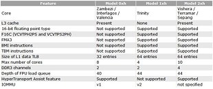
CPU World compiled most of the features of what it suspected to be AMD referring to its future processors based on the Piledriver architecture, that's "Vishera" (desktop high-performance), "Terramar" (high-density server), and "Sepang" (small-medium business server) parts. The three are not the first chips to be based on Piledriver, AMD has a new mainstream desktop and notebook APU in the works codenamed "Trinity", which is en route for a little later this year. Trinity basically has an identical CPUID instruction-set as Vishera, Terramar, and Sepang, confirming their common lineage compared to today's "Bulldozer" architecture. The most catchy detail is of Vishera featuring 4 DDR3 channels.

TYAN Announces an Array of AMD Opteron 6200 and 4200 Series Processor Platforms

TYAN, an industry-leading server platform manufacturer and a subsidiary of MiTAC International Corp., will announce its latest platforms that fully support the latest 32nm AMD Opteron 6200 and 4200 Series processors (NYSE: AMD) at SC11. TYAN will be presenting a live demo of its GN70-B8236-IL, a powerful and cost-effective GPU/HPC 2U server solution installed with two AMD Opteron 6200 Series processors and two AMD FirePro V8800P Graphic Cards at TYAN booth #4202 during the show.

TYAN will be showcasing its broad portfolio featuring AMD Opteron 6200 and 4200 Series processors which ensure that customers experience power efficiency, performance, scalability and management flexibility via features such as AMD Turbo CORE technology and HyperTransport 3.0 Technology. TYAN offers a total of 13 AMD G34 solutions that support the 16-Core AMD Opteron 6200 Series processors which deliver advanced performance for complex workloads and offer flexible scalability for expanding HPC requirements. TYAN also offers six AMD C32 platforms which are compatible with AMD Opteron 4200 Series processors and target applications ranging from general purpose computing to highly-threaded mission-critical applications such as SMB cloud computing, web servers as well as VM applications and virtual machines.

AMD FX 8100 Surfaces on HP Pavilion Desktop

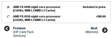
AMD's third 8-core desktop processor model is available through OEMs such as HP. Called the AMD FX-8100, this chip is the most affordable among the available FX-8000 series chips (that's FX-8120 and FX-8150), and according to HP's component pricing, about $80 cheaper than the FX-8150. The AMD FX-8100 is a base model processor option for HP Pavilion HPE h8z desktop. It can be configured to have FX-8150 instead, for $80 over the base price of the desktop, of $830.

The FX-8100, like every other FX Series processor, features an unlocked base clock multiplier to help with overclocking. The chip is clocked at 2.80 GHz, with TurboCore technology, all eight cores can overclock themselves to 3.10 GHz. To handle tasks that aren't multi-threaded, the chip can overclock some of its cores (up to four of them), all the way up to 3.70 GHz. Like every other FX-8000 series chip, the FX-8100 packs 16 MB of total cache (8 MB total L2 + 8 MB L3), features an advanced instruction set of AVX, AES, XOP, SSE 4.2/4.1/4a, and a system interface of 5.2 GT/s with HyperTransport 3.1.

AMD Readies Opteron 4200 ''Valencia'' Line for 1P/2P Servers

In early September, AMD announced that it started shipping the first processors based on the "Bulldozer" architecture, in the enterprise-centric Opteron 6100 "Interlagos" family. Opteron 6100 chips are capable of 4P (four-socket) servers, and feature up to 12 cores. AMD isn't stopping at the Opteron 6100 series, it has a new line of Opteron processors based on the same "Bulldozer" architecture, that targets small and medium enterprises. The line is codenamed "Valencia", its parts are filed under the Opteron 4200 series.

Opteron 4200 "Valencia" consists of 6-core and 8-core parts in the s1207 package. These chips are capable of single socket and two socket (2P) server setups, because while Opteron 6100 "Interlagos" has four HyperTransport links, Opteron 4200 has just two, so a processor can use its two links to connect to the SR56x0 I/O hub and the other processor. Opteron 4200 series consists of four 8-core models: Opteron 4284, Opteron 4280, Opteron 4274HE, and Opteron 4256EE; and four 6-core models: Opteron 4238, Opteron 4234, Opteron 4228HE, and Opteron 4226.

AMD Paves the Way for the Next Gen. of Supercharged Desktop PCs with 9-Series Chipset

AMD today launched its 9-Series chipset line-up today, helping PC builders to develop next generation high performance desktop platforms. The company also unveiled its 2011 HD Tablet Platform, based on the AMD Z-Series Accelerated Processing Unit (APU), enabling vivid media display and content creation capabilities for the fast-growing market of Microsoft Windows-based tablets. These new AMD products are designed to enable more immersive digital experiences for the PC and tablet markets.

"As consumer appetites for more compelling, lifelike visual experiences increase, there is greater need for high performance, smooth, vibrant graphics as well as unparalleled computing power," said John Taylor, product marketing director, AMD. "From tablets to desktops, AMD is making powerful computing accessible to everyone."

ASUS 990FX Sabertooth Motherboard Pictured

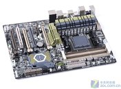
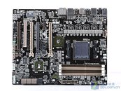
With the socket AM3+ platform, ASUS wants to rally around its top motherboard brands, including Republic of Gamers (ROG), with the ASUS Crosshair V Formula, and the The Ultimate Force (TUF) Sabertooth 990FX, for AMD's next top of the line 990FX chipset that is designed to run up to four discrete graphics cards. The 990FX Sabertooth keeps up with the color scheme of the other TUF-series members. It boasts of highly durable components. The AM3+ socket is powered by a 10-phase Digi+ VRM. It is wired to four DDR3 DIMM slots supporting dual-channel DDR3-1866 MHz memory, and connects to the 990FX chipset over a HyperTransport 3.1 link.

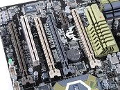
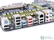
Expansion slots include four PCI-Express 2.0 x16 (configurable as x16/x4/x8/x8, x16/x4/x16/NC, depending on how they're populated); The electrical x4 slot is wired to the SB950 southbridge, and is placed there to hold PCI-Express SSDs. One each of PCI-E x1 and PCI make for the rest of the expansion. Storage connectivity includes six internal SATA 6 Gb/s ports supporting RAID, two internal SATA 3 Gb/s from a third-party controller, one power-eSATA/USB combo, and one normal eSATA on the rear panel.

AMD Intros Phenom II X4 980 Black Edition Quad-Core Processor

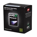
Today AMD released to market its latest quad-core processor, the Pheonom II X4 980 Black Edition. The new, faster SKU was first reported to be taking shape back in March. Based on the 45 nm "Deneb" silicon and K10.5 architecture, the X4 980 BE is yet another speed-bump, clocked at 3.70 GHz (18.5 x 200 MHz), with room for some overclocking thanks to its unlocked BClk multiplier.

The Deneb die packs four x86-64 cores with 512 KB caches each, and a shared 6 MB L3 cache. Despite its high clock speed, the processor maintains TDP of 125W. Its IMC supports dual-channel DDR3/DDR2 memory, and is backwards compatible with AM2+ socket apart from its native AM3 socket. HyperTransport 4 GT/s is its chipset interconnect. The new processor is priced at US $195.

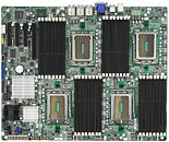
TYAN Launches Quad Socket G34 Server for AMD Opteron 6100 Series Processors

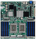
TYAN, an industry-leading server platform manufacturer, and a subsidiary of MiTAC International Corp., today launched a new 4U server system designed for CPU-intensive and HPC applications that supports four AMD Opteron 6100 series processors. TYAN offers both the 4-way S8812WGM3NR motherboard, as well as the B8821F48W8R server platform.

ZOTAC Unleashes Duo of AMD 800 Series Mini-ITX Platforms

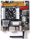
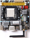
ZOTAC International, a leading innovator and the world's largest channel manufacturer of graphics cards, motherboards and mini-PCs, today unleashes a duo of mini-ITX platforms designed for optimal energy-efficiency, home theatre PC and powered by AMD 800 series chipsets - including the world's first AMD mobile-on-desktop platform - the new ZOTAC M880G-ITX WiFi - and the socket AM3 compatible 880G-ITX WiFi.

Powered by AMD 800 series chipsets, the ZOTAC M880G-ITX WiFi and 880G-ITX WiFi platforms deliver a premium AMD experience in a mini-ITX form factor with USB 3.0, SATA 6.0 Gb/s and 802.11n WiFi technologies. High-performance integrated ATI Radeon HD 4200 series graphics processor enables stunning visuals with Microsoft DirectX 10.1 technology.

Zambezi AM3+ Core Logic Slated for Q2-2011

AMD's upcoming "Bulldozer" architecture based processors that use a new socket type, the AM3+, are slated for Q2, 2011. To complement its launch, AMD will be launching the 9-series chipset series, consisting of four kinds of desktop chipset. The lineup starts with the AMD 990FX, the high-end 4-way CrossFireX-ready chipset, geared for high-end motherboards. Next up, is the 990X. This discrete graphics chipset is also ready for CrossFireX, but has just 16 PCI-Express 2.0 lanes to spare for graphics, platforms based on this will feature two PCI-Express x16 slots which reconfigure to electrical x8 slots when both are populated.

The third is an entry-level discrete graphics chipset that doesn't support CrossFire, but can spare one PCI-Express 2.0 x16 slot for discrete graphics, it's the AMD 970. Lastly, there's the 980G integrated graphics chipset, which features a DirectX 10.1 compliant IGP, which supports UVD 2.0 video acceleration. For some reason, this chipset doesn't support older AM3 processors, but only AM3+. The other chipsets in the series however, do support existing socket AM3 Athlon II and Phenom II series processors. All four northbridge chipsets support HyperTransport 3.0 processor interconnect, supporting data rates of up to 5.2 GT/s.

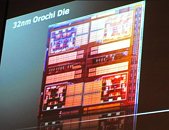
Bulldozer-based Orochi and Fusion Llano Die Shots Surface in GlobalFoundaries Event

The first official die-shots of the first Bulldozer architecture derivative, the eight-core "Orochi" Opteron die was displayed at Global Technology Conference, by GlobalFoundries, AMD's principal foundry-partner. While AMD did not give out a die-map to go with it, the structures we can make out are four Bulldozer modules holding two cores and a shared L2 cache each, a L3 cache spread across four blocks that's shared between all cores, the northbridge-portion cutting across the die at the center, and the integrated memory controller along its far-right side. Various I/O portions are located along the other three sides.

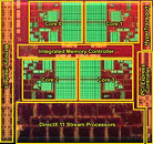
Next up is the Llano die. This is AMD's very first Fusion APU (accelerated processing unit) die. It is based on the K10 architecture and integrates a graphics processor and northbridge completely into one die. It precedes APUs based on the Bobcat architecture. Fortunately, there is a die-map at hand, which shows four K10 cores with dedicated 1 MB L2 caches per core, no L3 cache, an integrated SIMD array that holds 480 stream processors. The GPU component is DirectX 11 compliant. Other components include an integrated northbridge, integrated memory controller, integrated PCI-Express root complex, and HyperTransport interface to the chipset.

AMD Details Bulldozer Processor Architecture

AMD is finally going to embrace a truly next generation x86 processor architecture that is built from ground up. AMD's current architecture, the K10(.5) "Stars" is an evolution of the more market-successful K8 architecture, but it didn't face the kind of market success as it was overshadowed by competing Intel architectures. AMD codenamed its latest design "Bulldozer", and it features an x86 core design that is radically different from anything we've seen from either processor giants. With this design, AMD thinks it can outdo both HyperThreading and Multi-Core approaches to parallelism, in one shot, as well as "bulldoze" through serial workloads with a broad 8 integer pipeline per core, (compared to 3 on K10, and 4 on Westmere). Two almost-individual blocks of integer processing units share a common floating point unit with two 128-bit FMACs.

AMD is also working on a multi-threading technology of its own to rival Intel's HyperThreading, that exploits Bulldozer's branched integer processing backed by shared floating point design, which AMD believes to be so efficient, that each SMT worker thread can be deemed a core in its own merit, and further be backed by competing threads per "core". AMD is working on another micro-architecture codenamed "Bobcat", which is a downscale implementation of Bulldozer, with which it will take on low-power and high performance per Watt segments that extend from all-in-One PCs all the way down to hand-held devices and 8-inch tablets. We will explore the Bulldozer architecture in some detail.

ASUS Readies AMD-based Eee PC 1015T Netbook

ASUS' Eee PC series of netbooks is finally going to get an AMD-based model, the 1015T. This 10.1 inch netbook has a 1024 x 600 pixel screen, and is driven by an AMD V105 single-core processor based on the K8 architecture. The V105 is a 45 nm based processor with 1.20 GHz clock speed, HyperTransport 2 GT/s system interface, 128 KB of L1 and 512 KB of L2 cache, and a TDP of 9W. The processor is accompanied by RS880 chipset, with integrated ATI Radeon HD 4200 graphics. The 1015T packs 512 MB of memory, 250 or 320 GB HDD with 500 GB of web-based storage, 802.11 b/g/n WiFi, Bluetooth 3.0 (optional), and a battery with up to 6 hours of operation on a full-charge. There is no word on its pricing.
Return to Keyword Browsing
Nov 21st, 2024 11:37 EST change timezone

New Forum Posts

Popular Reviews

Controversial News Posts