Inside "Arrow Lake": Intel's Die Exposed and Annotated
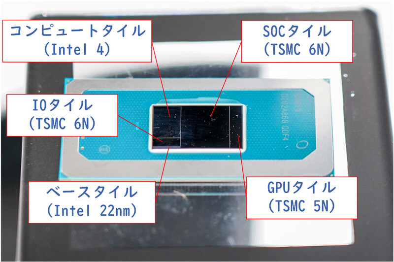
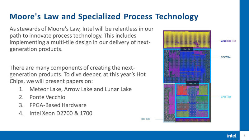
Die shots of Intel's "Arrow Lake" desktop processors have appeared online, confirming the chiplet design we have known about since the launch. The images annotated by the YouTube channel HighYield show a four‑tile arrangement mounted on a base die made with Intel's 22 nm FinFET process. The compute tile sits at the top left, built on TSMC's N3B node and covering 117.24 mm². To its right are the SoC tile on TSMC's N6 node measuring 86.65 mm², and the GPU tile, which houses four Xe cores alongside an Arc Alchemist render slice. The I/O tile, at 24.48 mm² on the same N6 node, completes the group at the bottom left. Intel has redesigned its hybrid core layout for Arrow Lake, moving away from separate P‑core and E‑core clusters. Four of the eight high‑performance P‑cores line the die's outer edges, with the remaining four in the center. In between these lie the four efficiency E‑core clusters, each sharing 3 MB of L2 cache. A unified 36 MB L3 cache ring bus connects to every core, allowing E‑cores to tap into that larger cache pool for the first time. Intel aims to spread heat more evenly and boost background task performance.
The I/O tile integrates Thunderbolt 4 controllers, PCIe buffers and PHYs. The SoC tile carries display engines, media accelerators and DDR5 memory controllers. All tiles are bonded to the base die via Intel's Foveros Omni stacking technology. Arrow Lake also reflects a shift in Intel's manufacturing strategy. Plans to use Intel's 20A node were dropped in favor of TSMC processes, making this the first desktop CPU from Intel that relies almost entirely on external foundries. On the software side, Intel has begun offering its IPO profiles in select prebuilt systems. These presets optimize CPU and memory settings for a hassle‑free performance boost that remains within warranty limits. Meanwhile, the native 200S Boost overclocking option is rolling out via BIOS updates. Early tests suggest that 200S Boost alone yields modest gains unless paired with very high-speed DDR5 modules, while IPO profiles deliver more consistent improvements with mainstream memory configurations.


The I/O tile integrates Thunderbolt 4 controllers, PCIe buffers and PHYs. The SoC tile carries display engines, media accelerators and DDR5 memory controllers. All tiles are bonded to the base die via Intel's Foveros Omni stacking technology. Arrow Lake also reflects a shift in Intel's manufacturing strategy. Plans to use Intel's 20A node were dropped in favor of TSMC processes, making this the first desktop CPU from Intel that relies almost entirely on external foundries. On the software side, Intel has begun offering its IPO profiles in select prebuilt systems. These presets optimize CPU and memory settings for a hassle‑free performance boost that remains within warranty limits. Meanwhile, the native 200S Boost overclocking option is rolling out via BIOS updates. Early tests suggest that 200S Boost alone yields modest gains unless paired with very high-speed DDR5 modules, while IPO profiles deliver more consistent improvements with mainstream memory configurations.